Explore the key features and internal architecture of the Intel 8086 microprocessor, including its design, functionality, and components. Learn about the Bus Interface Unit (BIU), Execution Unit (EU), and the significance of instruction queues in optimizing program execution.
Please find below an Image/Link to download the presentation.
The content on the website is provided AS IS for your information and personal use only. It may not be sold, licensed, or shared on other websites without obtaining consent from the author. If you encounter any issues during the download, it is possible that the publisher has removed the file from their server.
You are allowed to download the files provided on this website for personal or commercial use, subject to the condition that they are used lawfully. All files are the property of their respective owners.
The content on the website is provided AS IS for your information and personal use only. It may not be sold, licensed, or shared on other websites without obtaining consent from the author.
What is Microprocessor? "Microprocessor is a programmable electronic device that controls interpretation and execution of the instructions. It is called as CPU of the computer". The word micro in the microprocessor refers to its small size and the processor refers to the device that performs computational and control operations.
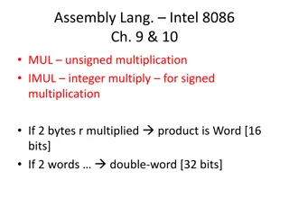
Salient features of 8086 The Intel 8086 is a 16-bit microprocessor. It contains approximately 29,000 transistors. The number of address pins is 20 and hence the memory addressing capacity is 220= 1 megabyte. The 8086 has 20 address pins, 16 of which are also used as data pins. The use of pins for both addresses and data means that both an address and datum cannot be sent to the system bus at the same time. This multiplexing of addresses and data reduces the number of pins needed, but does slowdown. Rounding out the 40-pinconfiguration are two grounds. The 8086 requires only one supply voltage, + 5 V, and one clock phase whose frequency can be up to 5 MHz. There are 16 control lines for various control operations. 1. 2. 3. 4. 5. 6. 7. 8.
Bus Interface Units(BIU) It is responsible of transfer of instructions, addresses and data on the system bus to the execution unit. It handles the transfer of the data between the processor, memory and I/o devices. It includes instruction fetch, data fetch, address transfer and computation of effective address of the memory. The functional parts of BIU are, 1. Instruction Queue (IQ) 2. Segment Registers 3. Instruction Pointer (IP)
Instruction Queue The instruction queue is of six bytes in length and is used to speed up the execution of programs, by perfecting six instruction bytes in advance from the memory. The perfected instructions are stored in a group of high speed registers known as the INSTRUCTION QUEUE. The BIU(Bus Interface Unit) works in parallel with the EU(Execution Unit). The BIU fetches the instruction bytes while the EU is executing an instruction. The process of fetching the next instruction in advance while the EU is executing the current PIPELINING. 1 2 6 bytes 3 4 5 6 instruction is known as
Segment Registers They are the additional 16-bit registers to generate memory address when combined with the other registers in the microprocessors. There are four segment registers. Code Segment Registers (CS) 1. Data Segment Registers (DS) 2. Stack Segment Registers (SS) 3. Extra Segment Registers (ES) 4.
Code Segment Register The code segment is a section of a memory that holds the code 1. (programs and procedures) used by the microprocessor. The CS register defines the starting address (Upper 16 bits of 2. the 20-bit starting address of the segment) of the section of memory holding code. The code segment is limited to 64 KB.
Data Segment Register The data segment is a section of memory that contains most 1. data used by a program. Data are accessed in the data segment by an offset address or the contents of other registers that hold the offset address. The data segment is limited to 64 KB. 2.
Stack Segment Register The stack segment defines the area of the memory used for the stack. The stack pointer (SP) determines the location of the current entry point in the stack segment. The BP register also addresses (Access) data with in the stack segment. .
Extra Segment Register The extra segment is an additional data segment used by some of the string instructions to hold the destination data. The extra segment is limited to 64 KB.
IP (Instruction Pointer) It is designated as IP. 1. 2. The instruction pointer, which points to the next instruction in a program, is used by the microprocessor to find the next sequential instruction in a program located with in the code segment. It is also called as program counter in the microprocessor. 3.
Execution Unit The execution unit works parallel with Bus Interface Unit 1. It informs the BIU the location at which the next instruction or data is to be fetched. 2. The instruction consists of different phases. i.e Fetch, Execute, Decode and Write phases. 3. The Fetch Phase performs the fetching of instructions. 4. The Execution Phase performs actual operation on data. 5. The Decode Phase perform the decoding of instructions. 6. The Write Phase performs the operation of storing the result at destination. 7.
The functional parts of EU are, Control system and Instruction Decode 1. Arithmetic and Logic Unit 2. Flag Register 3. General Purpose Registers 4. Stack Pointer Register 5. Pointer and Index registers 6.
Control system and Instruction Decode It directs all the internal operation of the processor. The instruction in the EU translate the instruction fetched from the memory into a series of actions carried out by the EU. 1. 2. Arithmetic and Logic Unit It is one of the components of EU. It performs 8-bit or 16-bit mathematical operations such as subtraction, multiplication, division, data conversion and logical operations like NOT, OR,AND. It also performs register increment and decrement and shift operations. 1. addition, 2. 3.
Flag Registers Processor Status Word (PSW): The register that holds current status of the processor. 1. 8086 s PSW contains 16 bits, but 7 of them are not used. Each bit in the 2. PSW is called a flag. Types of Flags Conditional Flag Control Flags
Auxiliary Carry Flag This is set, if there is a carry out of bit 3 during the addition or barrow by bit 3 during subtraction. Sign Flag Is equal to MSB of the result. Negative numbers have a1 in MSB and Non negative numbers then bit is Zero. Zero Flag Tarp Flag If this flag is set, the processor enters the single step execution mode by generating internal interrupts after the execution of each instruction Carry Flag This flag is set, if the result of the computation or performed by an instruction is zero This flag is set, when there is a carry out of MSB in case of addition or a borrow in case of subtraction. comparison Over flow Flag Parity Flag This flag is set, if an overflow occurs, i.e, if the result of a signed operation is large enough to accommodate in a destination register. The result is of more than 7-bits in size in case of 8-bit signed operation and more than 15- bits in size in case of 16-bit sign operations, then the overflow will be set. Direction Flag This is used by string manipulation instructions. If this flag bit is 0 , the string is processed beginning from the lowest address to the highest address, i.e., auto incrementing mode. Otherwise, the string is processed from the highest address towards the lowest address, i.e., auto incrementing mode. This flag is set to 1, if the lower byte of the result contains even number of 1 s ; for odd number of 1 s set to zero. Interrupt Flag If, set certain type of interrupt is recognised by the CPU, otherwise, these interrupts are ignored.
General Purpose Registers The 8086 processor has four 16- bit general purpose registers. They are, AX, BX, CX, DX Again it can be divided into the two 8-bit registers distinguished as high and low order bytes, referenced as AH, AL,BH, BL, CH, CL and DH, DL.
Accumulator Register (AX) Consists of two 8-bit registers AL and AH, which can be combined together and used as a 16-bit register AX. AL in this case contains the low order byte of the word, and AH contains the high-order byte. Multiplication and Division instructions also use the AX or AL.
Base Register (BX) Consists of two 8-bit registers BL and BH, which can be combined together and used as a 16-bit register BX. It is used holds the offset address of a location in the memory system.
Count Register (CX) Consists of two 8-bit registers CL and CH, which can be combined together and used as a 16-bit register CX. When combined, CL register contains the low order byte of the word, and CH contains the high-order byte. Instructions such as SHIFT, ROTATE and LOOP use the contents of CX as a counter.
Data Register (CX) It is a general purpose register that holds the port address during certain IN and OUT instruction.
Stack Pointer (SP) and Base Pointer (BP) Both SP and BP registers are 16- bit registers. The register SP points to the current stack of the stack. Where as BP points to the memory location for memory data transfers and also access the data within the stack segment.
Source Index (SI) and Destination Index (DI) Used in indexed addressing. Instructions that process data strings use the SI and DI registers together with DS and ES respectively in order to distinguish between the source and destination addresses.
Source Index (SI) and Destination Index (DI) Used in indexed addressing. Instructions that process data strings use the SI and DI registers together with DS and ES respectively in order to distinguish between the source and destination addresses.


")


")


")
")
")
")
 and Base Pointer (BP)")
 and Destination Index (DI)")
 and Destination Index (DI)")