Advanced 120GHz Imaging Radar Project Overview
Explore the innovative 120GHz millimeter wave imaging radar project led by a diverse team of professionals. The project aims to build a radar system based on the TRA_120_045 radar chip for non-destructive evaluation, flaw detection, and radar imaging experiments. Detailed designs and subsystems like RF boards, FPGA boards, and ADC boards are discussed, along with the system's conceptual sketches. Learn about the components/modules design, system architecture, and the project vision.

Download Presentation

Please find below an Image/Link to download the presentation.
The content on the website is provided AS IS for your information and personal use only. It may not be sold, licensed, or shared on other websites without obtaining consent from the author. If you encounter any issues during the download, it is possible that the publisher has removed the file from their server.
You are allowed to download the files provided on this website for personal or commercial use, subject to the condition that they are used lawfully. All files are the property of their respective owners.
The content on the website is provided AS IS for your information and personal use only. It may not be sold, licensed, or shared on other websites without obtaining consent from the author.
E N D
Presentation Transcript
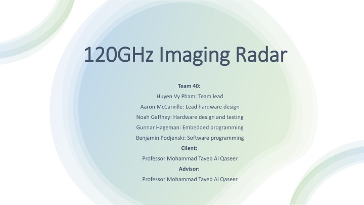
120GHz Imaging Radar 120GHz Imaging Radar Team 40: Huyen Vy Pham: Team lead Aaron McCarville: Lead hardware design Noah Gaffney: Hardware design and testing Gunnar Hageman: Embedded programming Benjamin Podjenski: Software programming Client: Professor Mohammad Tayeb Al Qaseer Advisor: Professor Mohammad Tayeb Al Qaseer
Project goal: It is to build a 120 GHz millimeter wave (mm-wave) imaging radar. The system will be based on TRA_120_045 radar chip. There are two subsystems in the radar: RF circuit (radar IC and phased-locked-loop (PLL) circuitry). ADC circuit with FPGA A GUI Usage: It is mainly used for the Non-destructive Evaluation do object imaging and flaw detection inside of model. Approach: Building and testing two subsystems (RF and ADC boards) separately. Programming the Alchitry Au to control peripheral IC's through SPI. Configuring the Alchitry Au to send ADC data to Host PC via USB. Building a PC application for user to communicate to the system. Testing the system as a whole for functionality. Using the system to conduct radar imaging experiments in the microwave lab at CNDE. Project Vision Project Vision
Conceptual/Visual Sketch Conceptual/Visual Sketch RF Board: Radar IC and PLL circuitry Control signal Control signal User Interface: Data transfer and display; control signal FPGA Board: SPI, UART, and FTDI/ USB communication Data Control Signal Data ADC Board: Low Pass Filter, Amplifier, and ADC Data
System Design System Design TRA 045 chip Antenna on chip Internal diagram
System Design System Design Detailed design (components/modules design) for RF Board The Phase Lock Loop circuitry Phase Lock Loop circuitry Reference frequency RF frequency X Low Pass filter VCO N Divider
System Design System Design Detailed design (components/modules design) for ADC Board IFIp IFI ADC IFIn IFQp IFQ ADC IFQn
System Design System Design Detailed design (components/modules design) for Signal Path Host PC Alchitry Au Control signal RF Board GUI UART IFI and IFQ data / Control SPI ARTIX 7 Control signal FTDI Chip JTAG USB 2.0 IFI and IFQ data ADC Board
System Design System Design User Interface Prototype Control signal FPGA Raw Data (IFI and IFQ)
HW/SW platforms, technology, frameworks, standards System Design System Design GUI software: Front-end: Django Framework. Webpage Hosting: Raspberry Pi using an Apache webserver. Embedded Programming: Xilinx platform, Vivado (Hardware) and Vitis (Software). Communication between PC and FPGA: FTDI. RF and ADC board: KiCad. Lens Modeling: CST software. Testing: Spectrum Analyzer.
Project Plan Project Plan Task Decomposition: ADC Board PCB and Schematic RF board (based on Evaluation bard) FPGA ADC Board Programming FPGA Research and Learning Connecting the Data Sequencing with RF subsystem and FPGA and GUI Programming GUI Programming Lens Modeling
Project Plan Project Plan Schedule/Milestones Schedule/Milestones Expected Completion Date Milestone Radar Board Design Task Completion 10/23/2023 9/23/2023 10/23/2023 1/26/2024 Schematic Design Layout Design 100% 100% 100% Radar Board Testing PLL on the board to be locked at a single frequency, and it is detected by Spectrum Analyzer 100% 11/10/2023 PLL on the board can sweep a range of frequency and can be detected by Spectrum Analyzer 100% 11/30/2023 Conducting imaging using the Radar Board with NIDAQ 100% 1/26/2024
Project Plan Project Plan Schedule/Milestones Schedule/Milestones Expected Completion Date Milestone ADC Board Design Task Completion 100% 100% 100% 2/9/2024 12/6/2023 2/9/2024 3/9/2024 Schematic Design Layout Design ADC Board Testing Testing the functionality: A signal generator will send a voltage sine wave is sent to the ADC board. The raw ADC data is collected by the FPGA and is plotted by the host to be compared to the original voltage sine wave 30% Integrating the ADC board and RF board 0% 3/23/2024
Project Plan Project Plan Schedule/Milestones Schedule/Milestones Expected Completion Date Milestone FPGA programing Task Completion 3/31/2024 2/10/2024 2/17/2024 3/10/2024 Sending and echoing commands through UART Communicating with the GUI through UART Sending and echoing commands through SPI 100% 100% 30% Sending commands to program PLL through SPI 3/23/2023 Sending commands to program ADC through SPI 3/31/2024 Sending commands to program the Amplifier 3/31/2024
Project Plan Project Plan Schedule/Milestones Schedule/Milestones Expected Completion Date Milestone GUI programing Task Completion 3/31/2024 2/10/2024 3/23/2024 3/31/2024 Communicating with the FPGA through UART Sending control data to PLL to FPGA Receiving data from the DAC through FPGA 100% Live updating the data on the GUI 3/23/2024 Using Raspberry Pi to host the GUI 3/23/2024 Design a cage for the product Lens design and print for the radar 50% 3/31/2024 100% 11/31/2023
Current Design Current Design
Getting data transferred from the GUI to the Amplifier through SPI Reading from the ADC using the FPGA Challenges and Challenges and Solutions Solutions
Overall progress: Following the timeline and making progress every week. Plan for the remaining of the project: Focus more on FPGA programing and GUI. Targeting completion date: March 31st Summary Summary