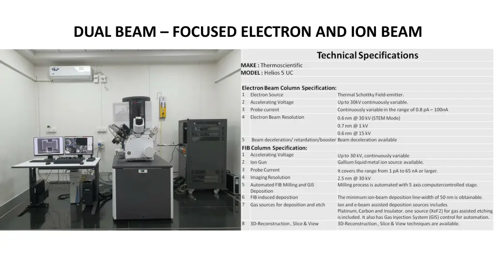
Advanced Materials Analysis and Imaging Services
Explore a range of advanced materials analysis and imaging services offered, including dual-beam FIB techniques for sample preparation, STEM imaging, EDS characterization, and nano-patterning. Services cover a variety of samples such as interstitial steel, TiO2/SiO2, Ni on pyramidal Si, and more. Benefit from state-of-the-art equipment like HR-TEM 300 kV Tecnai G2 F30 for precise analysis and imaging. Get insights into sample structures, grain boundaries, and interface properties. Dive into image analysis on the dual-beam FIB system, revealing intricate details of materials like Tin balls on Carbon, Au on Ag Nano Forest, and more.

Uploaded on | 1 Views
Download Presentation

Please find below an Image/Link to download the presentation.
The content on the website is provided AS IS for your information and personal use only. It may not be sold, licensed, or shared on other websites without obtaining consent from the author. If you encounter any issues during the download, it is possible that the publisher has removed the file from their server.
You are allowed to download the files provided on this website for personal or commercial use, subject to the condition that they are used lawfully. All files are the property of their respective owners.
The content on the website is provided AS IS for your information and personal use only. It may not be sold, licensed, or shared on other websites without obtaining consent from the author.
E N D
Presentation Transcript
Sample : Interstitial steel Required information : To study grains and grain boundaries in the sample Lamella Preparation, Thinning and STEM imaging using FIB at SAIF
Lamella analysis using TEM Imaging and EDS Characterization (HR-TEM 300 kV, Tecnai G2, F30 at SAIF)
Sample : TiO2/SiO2 Required information : To study alternate multilayers of TiO2 and SiO2 Lamella Preparation, Thinning and STEM imaging and EDS analysis using FIB at SAIF
Sample 3 : Ni on Pyramidal Si Required information : To check if oxide is present at the Ni - Si interface Lamella Preparation, Thinning and STEM imaging and EDS analysis using FIB at SAIF
NANO PATTERNING for Optical lenses on gold and Titanium Micro rings and holes on Titanium Nano Patterning on Au using FIB
IMAGE ANALYSIS on the Dual beam-FIB at SAIF Tin balls on Carbon Mesoporous Silica Au on Carbon Au on Ag Nano Forest