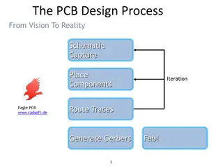
Advanced PCB Layout Techniques for Signal and Ground Routing
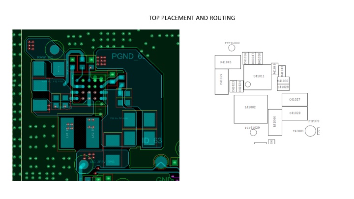
Explore different layers of PCB design, from top placement and routing to ground vias for signal integrity. Learn strategies for optimizing signal paths and maximizing grounding effectiveness. Enhance your PCB layout skills with advanced techniques for high-performance electronics.

Download Presentation

Please find below an Image/Link to download the presentation.
The content on the website is provided AS IS for your information and personal use only. It may not be sold, licensed, or shared on other websites without obtaining consent from the author.If you encounter any issues during the download, it is possible that the publisher has removed the file from their server.
You are allowed to download the files provided on this website for personal or commercial use, subject to the condition that they are used lawfully. All files are the property of their respective owners.
The content on the website is provided AS IS for your information and personal use only. It may not be sold, licensed, or shared on other websites without obtaining consent from the author.
E N D