Explore effective placement and routing strategies in electronic design, including principles for optimal cell arrangement, methods for simulated annealing cell swaps, and the RCT framework for resource, congestion, and timing optimization. Gain insights into critical considerations such as pin connections, I/O pins, and meeting specific timing requirements.
Please find below an Image/Link to download the presentation.
The content on the website is provided AS IS for your information and personal use only. It may not be sold, licensed, or shared on other websites without obtaining consent from the author. If you encounter any issues during the download, it is possible that the publisher has removed the file from their server.
You are allowed to download the files provided on this website for personal or commercial use, subject to the condition that they are used lawfully. All files are the property of their respective owners.
The content on the website is provided AS IS for your information and personal use only. It may not be sold, licensed, or shared on other websites without obtaining consent from the author.
E N D
Presentation Transcript
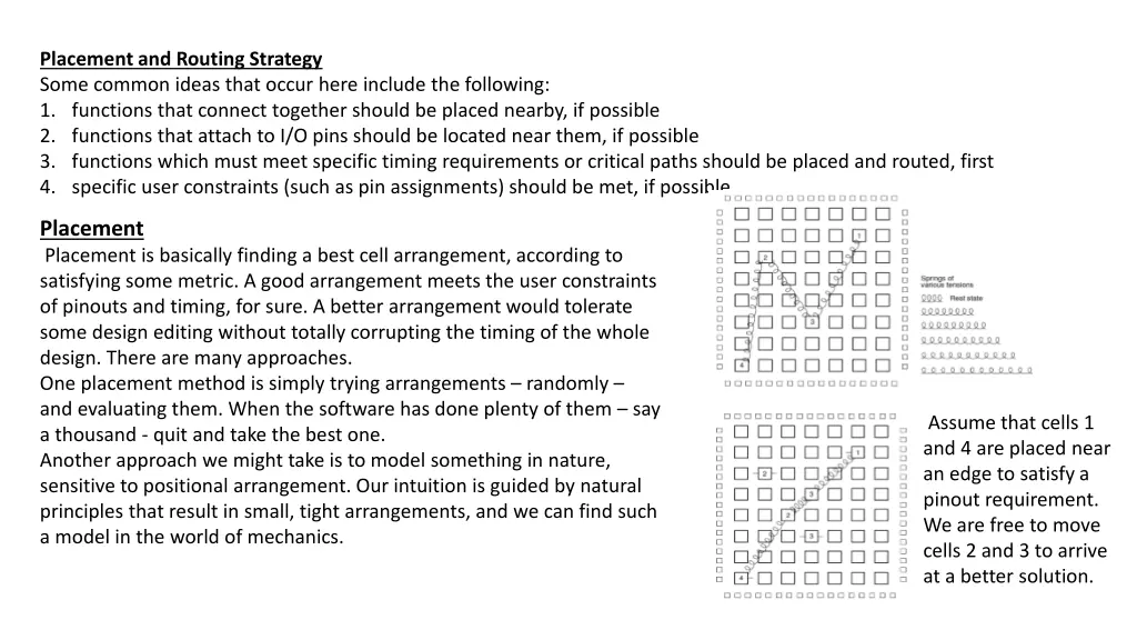
Placement and Routing Strategy Some common ideas that occur here include the following: 1. functions that connect together should be placed nearby, if possible 2. functions that attach to I/O pins should be located near them, if possible 3. functions which must meet specific timing requirements or critical paths should be placed and routed, first 4. specific user constraints (such as pin assignments) should be met, if possible Placement Placement is basically finding a best cell arrangement, according to satisfying some metric. A good arrangement meets the user constraints of pinouts and timing, for sure. A better arrangement would tolerate some design editing without totally corrupting the timing of the whole design. There are many approaches. One placement method is simply trying arrangements randomly and evaluating them. When the software has done plenty of them say a thousand - quit and take the best one. Another approach we might take is to model something in nature, sensitive to positional arrangement. Our intuition is guided by natural principles that result in small, tight arrangements, and we can find such a model in the world of mechanics. Assume that cells 1 and 4 are placed near an edge to satisfy a pinout requirement. We are free to move cells 2 and 3 to arrive at a better solution.
Placement Placement is basically finding a best cell arrangement, according to satisfying some metric. Figure 4-6 shows five successive versions of a set of placed cells. #1: is the random initial placement. #2: represents the situation after swapping the upper rightmost cell, with a blank to its lower left. I am using the spring process of lower energy, to guide the choices. #3: swaps the upper left cell down, by exchanging it with a blank that is nearer to the geometric center of the cluster. Here, we see a balanced looking set of five cells. #4: swaps the lower right cell with an adjacent blank that is above it. #5: exchanges the lower left cell with a blank above it, resulting in cluster shown. This might be a valid stopping point, as the cells are pretty much as close to each other, as can be permitted. #6: may or may not have merit, exchanging the blank in the top row of the cluster, with the cell in the top right of the cluster. We arbitrarily choose to stop here, as we envision no particularly better arrangement than this one. Figure 4-6 Five Simulated Annealing Cell Swaps
RCT Resource, Congestion and Timing The Virtex 4 ASMBL architecture introduced some architecture changes that suggested additional methods might be used for effective place and route. RCT is the framework that evolved to fit those needs. The RCT methodology is currently being successfully used. A key idea here is that the router should attempt to first optimize every connection required, by simply making the connection. This should give the fastest connection evaluation for all paths, for a given placement. After the paths have been connected, the design is analyzed to identify connection conflicts (read: short circuits). When conflicts are identified, a negotiation process is engaged, where cost is evaluated for all contenders in the conflict. The negotiation is designed to favor the net that requires the connection to make its timing budget. This process is termed overlap removal. Overlap removal can be viewed in general as a priority based negotiation process. Figure 4-10 Direct Routing, with Shorts Reading 3: Watch Cross Clock Domain Checking (CDC) video Figure 4-9 shows four different connection possibilities to connect points A-C, B-E, F-D.
SelectIO, DCI and ChipSync SelectIO The original Virtex supported about 16 different voltage standards. Virtex 7 supports about 60. A lot has happened since the initial introduction of Virtex FPGA devices, as technology has collapsed its transistor sizes and voltage levels. See Table 11-1. IO Standard Virtex 7 series. Ex: Voltages: 5V, 3.3V, 2.5V, 1.8V, 1.5V, 1.38V (1.03V L, 350mV), . Digitally Controlled Impedance (DCI) Digitally Controlled Impedance (DCI) is the capability for an I/O pin to be selfterminating, without requiring external resistor packs. This is important, because it is very difficult to get just the right impedance physically close enough to the I/O pins of large pin count packages, to be most effective. This patented circuitry is unique to Xilinx, and has found its way into the hearts and minds of thousands of designers ChipSync In order to distinguish the I/O voltage, impedance and drive capability from the other timing based features, the ChipSync title was created for the additional advanced capabilities present in Virtex 4. The roots can be seen in XC4000 FPGA devices and early Virtex FPGA devices that included input delay selection as an option. ChipSync includes Idelay, Bitslip, ISERDES and OSERDES capabilities. ChipSync makes interfacing to DDR SDRAM and QDR-II SRAM substantially easier than before.
Setup, Hold Time, Propagation Delay and Clock Frequency in an FPGA Setup time, hold time, and propagation delay all affect your FPGA design timing. The FPGA tools will check to make sure that your design meets timing, which means that the clock is not running faster than the logic allows. The minimum amount of time allowed for your FPGA clock (its Period, which is represented by T) can be calculated. tclk (min)= tsu+ th+ tLOGIC = T F = 1/T Generally in FPGA design, tsuand thare fixed, the only variable that need to control is tpor the Propagation Delay which represents how much tasks to be accomplished in one clock cycle. The more task to do, the longer tpresults in the higher tclk (min)which means that the clock for FPGA design is slower. This is the fundamental trade-off of FPGA designs. Setup time is the amount of time required for the input to a Flip-Flop to be stable before a clock edge. Hold time is the minimum amount of time required for the input to a Flip-Flop to be stable after a clock edge. Propagation Delay is the amount of time it takes for a signal to travel from a source to a destination.
Equations and impacts of Equations and impacts of setup Setup time is defined as the minimum amount of time BEFORE the clock s active edge by which the data must be stable for it to be latched correctly. Any violation in this required time causes incorrect data to be captured and is known as a setup violation. Hold time is defined as the minimum amount of time AFTER the clock s active edge during which the data must be stable. Any violation in this required time causes incorrect data to be latched and is known as a hold violation. setup and hold time and hold time At t = 0, FF1 is to process D2 and FF2 is to process D1. Time for D2 FF2, counting from the clock edge at FF1 is t1 = Tc2q+Tcomb For FF2 to successfully latch it, this D2 has to be maintained at D of FF2 for Tsetuptime before the clock tree sends the next positive edge of the clock to FF2. Hence to fulfill the setup time requirement, the equation should be like the following. Figure 2 Setup and hold timing diagram To avoid the hold violation at the launching flop, the data should remain stable for some time (Thold) after the clock edge. The equation to be satisfied to avoid hold violation looks somewhat like below: Tc2q+ Tcomb+ Tsetup Tclk+ Tskew------- (1) Tc2q+ Tcomb Thold+ Tskew------- (2) https://www.edn.com/design/systems-design/4392195/Equations-and-impacts-of-setup-and-hold-time
Pipeline Principle A non-pipelined system of combination circuits (A, B, C) that computation requires total of 300 picoseconds. Non-pipelined Diagram 100 ps 100 ps 100 ps OP1 Comb. logic A Comb. logic B Comb. logic C OP2 OP3 Time Cannot start new operation until previous one completes Delay = 300 ps / Throughput = 1/300 ps = 3.333 GOPS A pipelined version by adding register at each output of the combination circuits. Additional 20 picoseconds to save result in register. Begin new operation every 120 ps. Overall latency increases. Pipelined Diagram 100 ps 20 ps 100 ps 20 ps 100 ps 20 ps A B C OP1 A B C OP2 Comb. logic A R e g Comb. logic B R e g Comb. logic C R e g A B C OP3 Time Up to 3 operations in process simultaneously Clock Delay = 3x120 ps = 360 ps / Throughput = 1/120 ps = 8.33 GOPS
Non-uniform delays 50 ps 20 ps 150 ps 20 ps 100 ps 20 ps R e g Comb. logic B R e g Comb. logic C R e g Comb. logic A Delay = 3x170 ps = 510 ps Throughput = 1/170 ps = 5.88 GOPS slowest stage Clock OP1 A B C OP2 A B C OP3 A B C Time Throughput limited by slowest stage (170 ps) Other stages sit idle for much of the time Challenging to partition system into balanced stages www.cs.cmu.edu/afs/cs/academic/class/15349-s02/lectures/class4-pipeline-a.ppt
Pipelined Methodlogy Focus on placing pipelining registers around the slowest combination circuits. 1. Select one endpoint as an origin. 2. Draw a line that cross every output in the circuit. 3. Continue to draw new line from the origin across various circuit connevtions such that these new lines partition the inputd from the out puts. 4. Adding pipeline register at every point where a seperationg line crosses a connection will always generate a vavild pieline. Note: Ideal pipeline registers have zero delay, and zero setup/hold time. Non-pipeline Delay = 20 ns Throughput = 1/20 ns = 50 MOPS Non-pipeline Delay = 8 ns Throughput = 1/8 ns = 125 MOPS Origin
Pipelined Design Operation Pipelining is a process which enables parallel execution of program instructions. In FPGAs, this is achieved by arranging multiple data processing blocks in a particular fashion. For this, we first divide our overall logic circuit into several small parts and then separate them using registers (flip-flops). An Example: Let's take a look at a system of three multiplications followed by one addition on four input arrays. Our output yiwill therefore be equal to (ai bi ci) + di. Non-Pipelined Design The first design that comes to mind to create such a system would be multipliers followed by an adder, as shown in Figure 2a. Figure 2a. An example of non-pipelined FPGA design. Image created by Sneha H.L. .
Pipelined Design Operation Now, let's suppose that we add registers to this design at the inputs (R1through R4), between M1and M2(R5and R8, respectively) and along the direct input paths (R6, R7, and R9), as shown by Figure 3a. Figure 3a. An example of pipelined FPGA design. Image and table created by Sneha H.L.
Consequences of Pipelining Latency: In the example shown, pipelined design is shown to produce one output for each clock tick from third clock cycle. This is because each input has to pass through three registers (constituting the pipeline depth) while being processed before it arrives at the output. Similarly, if we have a pipeline of depth n, then the valid outputs appear one per clock cycle only from nthclock tick. The greater the number of pipeline stages, the greater the latency that will be associated with it. Increase in Operational Clock Frequency The non-pipelined design is shown to produce one output for every three clock cycles. For T = 1 ns, takes 3ns. This longest data path would then be the critical path, which decides the minimum operating clock frequency of our design. In other words, the frequency F (1/3 ns) = 333.33 MHz. In the pipelined design, once the pipeline fills, there is one output produced for every clock tick or F 1/1ns = 1000 MHz. Increase in Throughput A pipelined system can increase the throughput of an FPGA. Greater Utilization of Logic Resources In pipelining, we use registers to store the results of the individual stages of the design. These components add on to the logic resources used by the design and make it quite huge in terms of hardware. Conclusion The act of pipelining a design is quite exhaustive. You need to divide the overall system into individual stages at adequate instants to ensure optimal performance. Nevertheless, the hard work that goes into it is on par with the advantages it renders while the design executes.
Reduce Cycle Time by Retiming Reduce Area by Retiming FF count = 9 External behavior unchanged FF count = 8 Moving register position leads to reduce FF counts (cycle time unchanged) Moving register position leads to balancing of delays
a) Identify the shortest FF to FF path to be considered when evaluating the hold requirement for the FF. Mark the path on the diagram. If several paths tie identify one. Can this circuit operate? Show how you determine this. b) Identify the longest FF to FF path to be considered when evaluating the setup requirement for the FF. Mark the path on the diagram. If several paths tie identify one. Assume the circuit operates, what is the minimum clock period? Show how you determine this. Solution: a) 4 tie. Tq + Tg2 + Tg2 + Tg2 Th 2 + 2 + 2 + 2 = 8 ns 8.5 ns ? No. Not working b) 3 tie. Tq + Tg3 + Tg2 + Tg2 + Tg2 + Tg2 + Tsu = Tmin 2 + 3 + 2 + 2 + 2 + 2 + 23 = 36 ns Tmin = 36 ns Fmax = 27.77 MHz


 Identify the shortest FF to FF path to be considered")