Analog Circuit Design for Low-Voltage Cascode Current Mirrors
Explore the design problems and specifications related to low-voltage cascode current mirrors in analog circuit design. Analyze circuits, transistor characteristics, and operational amplifier configurations to meet input and output voltage requirements, input and output resistances, current gain, and more.

Download Presentation

Please find below an Image/Link to download the presentation.
The content on the website is provided AS IS for your information and personal use only. It may not be sold, licensed, or shared on other websites without obtaining consent from the author. If you encounter any issues during the download, it is possible that the publisher has removed the file from their server.
You are allowed to download the files provided on this website for personal or commercial use, subject to the condition that they are used lawfully. All files are the property of their respective owners.
The content on the website is provided AS IS for your information and personal use only. It may not be sold, licensed, or shared on other websites without obtaining consent from the author.
E N D
Presentation Transcript
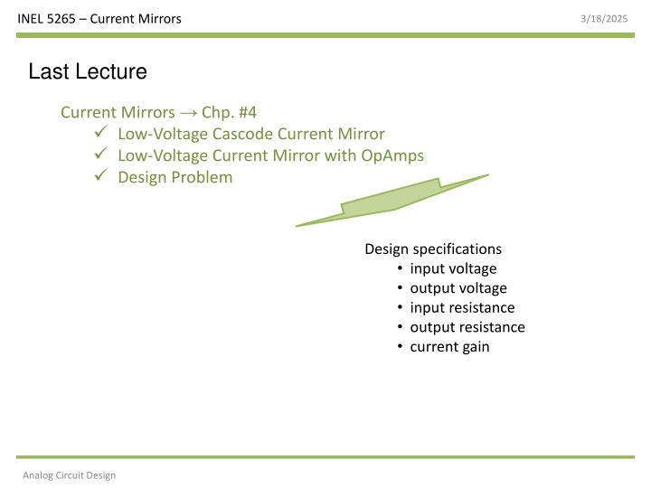
INEL 5265 Current Mirrors 3/18/2025 Last Lecture Current Mirrors Chp. #4 Low-Voltage Cascode Current Mirror Low-Voltage Current Mirror with OpAmps Design Problem Design specifications input voltage output voltage input resistance output resistance current gain Analog Circuit Design
INEL 5265 Current Mirrors 3/18/2025 Problem #1 -b Using the (W/L)s obtained part I, does de cascode current mirror still behaves properly for Rbias=40k ? Justify you answer. Vdd Vdd M10 M11 Vdd=3.3V M12 Vdd Vb Vdd M13 Iref Vdd Vout Iout Iref Vx Vy Vin M8 M4 M3 Ibias M9 Rbias M1 M7 Ibias M2 M6 M5 2 Analog Circuit Design
INEL 5265 Current Mirrors 3/18/2025 Problem #1 -c Assuming Ibias=10uA, and Vb=1.8V, design transistors M6-13 such that |Av|>30V/V Output Voltage Range = 1.3V Vdd Vdd M10 M11 Vdd=3.3V M12 Vdd Vb Vdd M13 Iref Vdd Vout Iout Iref Vx Vy Vin M8 M4 M3 Ibias M9 Rbias M1 M7 Ibias M2 M6 M5 3 Analog Circuit Design
INEL 5265 Current Mirrors 3/18/2025 Problem #1 -d Using the (W/L)s obtained on part III, find the possible voltage range for Vb such that the circuit still behaves properly. Vdd Vdd M10 M11 Vdd=3.3V M12 Vdd Vb Vdd M13 Iref Vdd Vout Iout Iref Vx Vy Vin M8 M4 M3 Ibias M9 Rbias M1 M7 Ibias M2 M6 M5 4 Analog Circuit Design
INEL 5265 Current Mirrors 3/18/2025 Homework #2 Design the cascode current mirror for the following specifications: Iout = 2 Iin=[0-10] A Vout(min) < 0.5V Vin < 0.9V VDD Iin Iout Ibias 1. 2. M2=2 M1 Vout(min)=Vds1(sat)+Vds2(sat) = 0.5V Choose Vds1(sat)=Vds2(sat)=0.25V Find W/L for M4,M2, and M1 Vin(max)=Vgs1=Vton+Vds1(sat)=0.95V does not satisfy Vds1(sat)=0.2V in order to satisfy Find new W/L for M1 and M2 Vgs3=Vgs4+Vds2(sat) Vds3(sat)=Vds4(sat)+Vds2(sat)=0.45V Find W/L for M3 + M3 M4 3. Vout 4. M1 M2 _ 5 Analog Circuit Design


