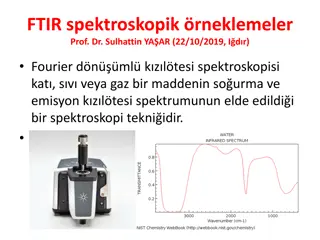
Applications of FTIR Testing in Semiconductor Industry
FTIR testing is widely used in semiconductor facilities for various applications such as centralized abatement system testing, performance efficiency testing, and quantifying total mass emissions. This method is capable of measuring a wide range of pollutants with low detection limits, making it suitable for characterizing semiconductor emissions. However, there are limitations and proper uses to consider, including the need for expertise to ensure quality results and understanding the detection limits for different compounds.

Download Presentation

Please find below an Image/Link to download the presentation.
The content on the website is provided AS IS for your information and personal use only. It may not be sold, licensed, or shared on other websites without obtaining consent from the author.If you encounter any issues during the download, it is possible that the publisher has removed the file from their server.
You are allowed to download the files provided on this website for personal or commercial use, subject to the condition that they are used lawfully. All files are the property of their respective owners.
The content on the website is provided AS IS for your information and personal use only. It may not be sold, licensed, or shared on other websites without obtaining consent from the author.
E N D
Presentation Transcript
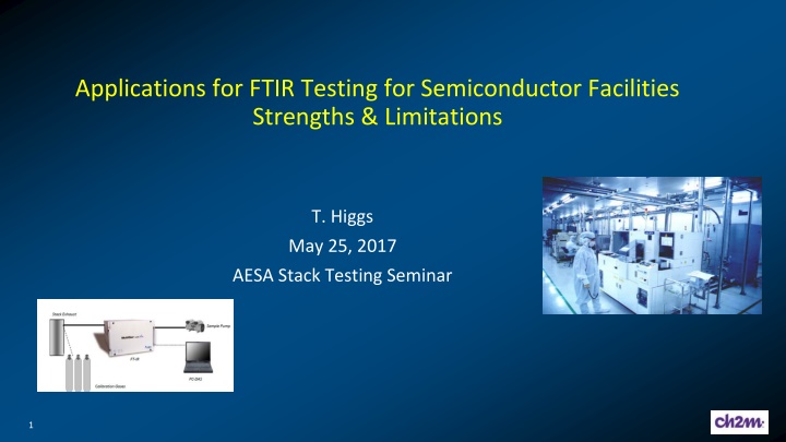
Applications for FTIR Testing for Semiconductor Facilities Strengths & Limitations T. Higgs May 25, 2017 AESA Stack Testing Seminar 1
Potential Applications FTIR testing widely used in semiconductor industry Centralized abatement system testing Performance efficiency testing, quantifying total mass emissions Scrubber systems Thermal oxidizers/VOC abatement Fab process tool characterization Plasma tools on etch/CVD operations Lithography tools Point of use abatement device performance 2
Pollutants of Interest Semiconductor fabs have diverse mix of pollutant types Hazardous Air Pollutants (HAPs) Hydrofluoric Acid (HF), Hydrochloric Acid (HCl), Chlorine (Cl2) Volatile Organic Compounds (VOCs) Speciation of individual organics sometimes desired (e.g. organic HAPs) Greenhouse gases Fluorinated gases (e.g. NF3, CF4, SF6) Nitrous oxide (N2O) Combustion sources (CO, NOx) 3
Semiconductor Emissions Characteristics Semiconductor fab emissions characterized by: Large number of individual emission generating units Hundreds of individual fab tools, connected to common exhaust systems Some tools emit multiple pollutants, pollutant types Separate exhaust systems - VOCs, acids, ammonia/bases Complex mix of pollutants in some exhaust systems High flow, relatively low concentration FTIR a good fit for fab emissions measurement Capable of measuring wide range of pollutants Low detection limits achievable on many 4
Exhaust System Layout Fab tools connecting into common main duct which branches off to several units 5
Proper Uses, Limitations for FTIR in SC Industry FTIR ideal for many testing needs - must understand limits, uncertainties Cl2, F2 emissions common in industry; not measurable by FTIR Detection limits vary by compound, conditions ND readings can have material impact on results in high flow systems VOC abatement efficiency best measured by total hydrocarbon method Emissions variability important if using short term test to quantify longer term emissions e.g. monthly, annual Interferences between compounds in complex exhaust stream High level of FTIR expertise needed to ensure quality results 6
Process Tool Emissions Testing Emissions out; may be - HAPs (e.g. HF) - GHGs (e.g. CF4, NF3) - VOCs Chemicals, gases in Typical flow rates may be 10 100 liters/minute Pollutant concentrations often > 100 ppm On any given tool, known list of possible pollutants is relatively small FTIR widely used for quantifying fab tool emissions Often compared to chemical use to understand use/emissions relationship and scale results to more tools, longer time periods 7
Point of use device testing Fab Tool Emissions in - Relatively high concentration, low flow - Short list of known pollutants Many emissions reduced >95% - Others converted to different materials, then treated - E.g. CF4, NF3 HF Simultaneous FTIR inlet/outlet testing often used to measure device removal efficiency 8
Quantifying annual HF Emissions from Scrubber Stacks Data from 2 fab sites over many years Detection limits typically 100 200 ppb Individual stack concentrations range from ND to ~1ppm tpy 8 hr. test period; results scaled to estimate annual emissions Total system flows range from 300-800k cfm In this application, non-detect readings can be a source of uncertainty in results 9
Error in Total Mass Determination at Various Flows In high flow exhaust systems detection limit can significantly impact overall error in total mass emissions calculation Max uncertainty introduced at different flow rates and detection limits Tpy HF Scrubber flow, kcfm 10
Quantifying annual HCl Emissions from Scrubber Stacks Data from 2 fab sites over many years Detection limits 400 500 ppb Individual stack concentrations range from ND to ~600ppb Most stacks ND tpy 8 hr. test period; results scaled to estimate annual emissions Total system flows 300-800k cfm In this application, non-detect readings introduce a large uncertainty high detection limits, most readings non-detect 11
Quantifying annual GHG Emissions from Scrubber Stacks Lb./hr at 0 Lbs./ hr at MDL 1.53 0.25 0.35 Annual mtCO2e at 0 44,652 31 354 Annual mtCO2e at MDL 45,033 96 926 Site w/30 scrubber stacks Combined flow 534,000 cfm 7 PFCs/HFCs monitored, 8 hrs./stack 1.52 0.08 0.13 CF4 CH3F CH2F 2 C2F6 SF6 CHF3 NF3 Total Material Det Limit, ppb 3 64 56 44 6 6 29 % of readings below det. limit 43.7 91.3 88.1 63.6 49.2 74.8 70.5 CF4 CH3F CH2F2 C2F6 SF6 CHF3 NF3 1.71 0.52 0.08 0.45 2.28 0.67 0.11 0.75 82,878 46,901 4830 30,983 210,629 110,521 61,077 6701 38,959 263,313 Average: 236,971 mtCO2 Error range: +/- 26,342 (11%) 12
Impact of Sampling Times Emissions fluctuate over time, impact scaling of short term results to longer term estimate Group of scrubber stacks monitored for 5 days Max and min HF results calculated from various time periods Based on 95% CI around average measured value Conclusion: Scaling results over short test periods can introduce significant error 8 hr. test period only introduces variability of +/- 0.3 tpy compared to 5 day HF Tpy 13
VOC Abatement System Testing Total removal efficiency testing best done with total hydrocarbon method Typical outlet concentration <2ppm THC Much of that is methane Individual organics a subset of what remains; quantifying individual species difficult 10 years of quarterly FTIR VOC outlet data 10 organics, almost all readings ND; occasional detections of methanol, ethanol, IPA Methanol Ethanol IPA m-xylene o-xylene p-xylene Ethyl Lactate PGMEA NBUAC HMDS CONCENTRATION (ppm) (ppm) (ppm) (ppm) (ppm) (ppm) (ppm) (ppm) (ppm) (ppm) ND ND ND ND ND ND ND ND ND ND ND ND ND ND ND ND ND ND ND ND ND ND ND ND ND ND ND ND ND ND Speciated methods (e.g. FTIR) may be useful for troubleshooting system performance issues Identifying which compounds are poorly removed 14
Summary Semiconductor manufacturing emissions are complex and highly variable Wide range of different pollutants, many contributing sources Often dilute at final emission point; relatively high concentration at source Stack testing has multiple purposes Abatement device removal efficiency Characterizing emissions from individual process steps Determining plant wide mass emissions By individual chemical, or group of chemicals (e.g. total hydrocarbons) FTIR is powerful tool for complex emissions with wide range of chemicals Important to understand both strengths and limits on ability to draw conclusions 15