ASIC Specifications and Tests for DCD and Switcher Chips
Explore the detailed specifications and testing plans for DCD and Switcher ASIC chips including size, number of channels, radiation tolerance, power consumption, and more. Discover the remaining challenges to meet the specifications and proposed solutions for optimization.

Download Presentation

Please find below an Image/Link to download the presentation.
The content on the website is provided AS IS for your information and personal use only. It may not be sold, licensed, or shared on other websites without obtaining consent from the author. If you encounter any issues during the download, it is possible that the publisher has removed the file from their server.
You are allowed to download the files provided on this website for personal or commercial use, subject to the condition that they are used lawfully. All files are the property of their respective owners.
The content on the website is provided AS IS for your information and personal use only. It may not be sold, licensed, or shared on other websites without obtaining consent from the author.
E N D
Presentation Transcript
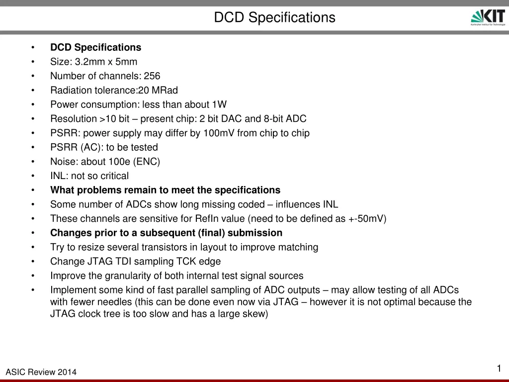
DCD Specifications DCD Specifications Size: 3.2mm x 5mm Number of channels: 256 Radiation tolerance:20 MRad Power consumption: less than about 1W Resolution >10 bit present chip: 2 bit DAC and 8-bit ADC PSRR: power supply may differ by 100mV from chip to chip PSRR (AC): to be tested Noise: about 100e (ENC) INL: not so critical What problems remain to meet the specifications Some number of ADCs show long missing coded influences INL These channels are sensitive for RefIn value (need to be defined as +-50mV) Changes prior to a subsequent (final) submission Try to resize several transistors in layout to improve matching Change JTAG TDI sampling TCK edge Improve the granularity of both internal test signal sources Implement some kind of fast parallel sampling of ADC outputs may allow testing of all ADCs with fewer needles (this can be done even now via JTAG however it is not optimal because the JTAG clock tree is too slow and has a large skew) 1 ASIC Review 2014
Switcher Specifications Switcher Specifications Size: Should fit to the bump pad pattern size of the chip may vary Number of channels: 32 Radiation tolerance: 20 MRad Power consumption: AC power consumption should dominate Switching speed: clear rise times should be about 10ns 20ns for 120pF (presently ~20ns) Voltage ranges: Amplitude up to 20V, High level: up to 30V (for clear), Low level: down to -10V (for gate) What problems remain to meet the specifications The CLEAR switching speed is slightly slower than simulated (now 20ns for 150pF load), however to my opinion DEPFET may work even with present raise times. More measurements are needed. Rise time increase is quite easy to implement larger output transistors Implement some kind of fast parallel sampling of switcher outputs 2 ASIC Review 2014
Switcher Tests Test plan for Switcher Important: should we implement extra test pads which are connected to JTAG and used only for testing: Motivation 1: testing of bump bond pads may damage them, motivation 2: test pads can be probed by standard needles Test JTAG (ID readout, readback) (if it does not work, do not use the chip) Test the operation with a suitable pattern for normal and gated mode readout, measure all outputs implement some kind of pattern recognition in FPGA (needs HV-LV converters) (only if pattern is correct in all the channels use the chip) (Alternative: implement HV-LV converter on chip load the data to JTAG chain) Use nominal voltages in the tests (Using of lower voltages may be ok to be discussed) 3 ASIC Review 2014
DCD Tests Test plan for DCD Important: should we implement extra test pads which are connected to JTAG and used only for testing: motivation 1: testing of bump bond pads may damage them, motivation 2: test pads can be probed by standard needles Test JTAG (ID readout, read-back, all digital IOs) (if it does not work, do not use the chip) Measure all ADC characteristics (every input 10 times) proposed by Christian Kreidl: measure the ADCs in parallel (8 in parallel) Comment: present needle card system does measurements at ~100MHz we need to improve the system to work at 320Mhz, one possibility: parallel sample of the digital signals are read in series Repeat the measurement for 2 RefIn voltages Estimation of the test time: (clocking out of all 64 outputs: 640ns) Number of points 2 (RefIn voltages) x 500 input current points x 10 repetitions x 32 ADCs x 640ns ~ 200 ms if FPGA does the test automatically data amount 2.56 MByte/chip: goal test one chip in 10 seconds Store the data as data base for offline analysis Offline analysis: make the score-table of all chips (e.g. by number of good ADCs) and start using from the best ones 4 ASIC Review 2014