Avalanche Photo Diodes: Understanding Semiconductor Materials
Learn about avalanche photo diodes (APDs) and how they utilize semiconductor materials like Silicon, Germanium, and InGaAs for light detection. Discover the principle, applications, and performance factors such as excess noise and quantum efficiency in APDs.

Download Presentation

Please find below an Image/Link to download the presentation.
The content on the website is provided AS IS for your information and personal use only. It may not be sold, licensed, or shared on other websites without obtaining consent from the author. If you encounter any issues during the download, it is possible that the publisher has removed the file from their server.
You are allowed to download the files provided on this website for personal or commercial use, subject to the condition that they are used lawfully. All files are the property of their respective owners.
The content on the website is provided AS IS for your information and personal use only. It may not be sold, licensed, or shared on other websites without obtaining consent from the author.
E N D
Presentation Transcript
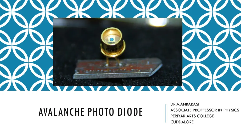
DR.A.ANBARASI ASSOCIATE PROFFESSOR IN PHYSICS PERIYAR ARTS COLLEGE CUDDALORE AVALANCHE PHOTO DIODE
AVALANCHE PHOTO DIODE In principle, any semiconductor material can be used as a multiplication region: Silicon will detect in the visible and near infrared, with low multiplication noise (excess noise). Germanium (Ge) will detect infrared out to a wavelength of 1.7 m, but has high multiplication noise. InGaAs will detect out to longer than 1.6 m and has less multiplication noise than Ge. It is normally used as the absorption region of a heterostructure diode, most typically involving InP as a substrate and as a multiplication layer.[3]This material system is compatible with an absorption window of roughly 0.9 1.7 m. InGaAs exhibits a high absorption coefficient at the wavelengths appropriate to high-speed telecommunications using optical fibers, so only a few micrometres of InGaAs are required for nearly 100% light absorption.[3]The excess noise factor is low enough to permit a gain-bandwidth product in excess of 100 GHz for a simple InP/InGaAs system,[4]and up to 400 GHz for InGaAs on silicon.[5]Therefore, high-speed operation is possible: commercial devices are available to speeds of at least 10 Gbit/s.[6] Gallium-nitride based diodes have been used for operation with ultraviolet light. HgCdTe-based diodes operate in the infrared, typically at wavelengths up to about 14 m, but require cooling to reduce dark currents. Very low excess noise can be achieved in this material system.
APD An avalanche photodiode (APD) is a highly sensitive semiconductor photodiode that exploits the photoelectric effect to convert light into electricity. From a functional standpoint, they can be regarded as the semiconductor analog of photomultipliers. The avalanche photodiode (APD) was invented by Japanese engineer Jun-ichi Nishizawa in 1952.[1]However, study of avalanche breakdown, microplasma defects in Silicon and Germanium and the investigation of optical detection using p-n junctions predate this patent. Typical applications for APDs are laser rangefinders, long-range fiber-optic telecommunication, and quantum sensing for control algorithms. New applications include positron emission tomography and particle physics. APD arrays are becoming commercially available, also lightning detection and optical SETI may be future applications.
NOISE AND QUANTUM EFFIENCY APplicability and usefulness depends on many parameters. Two of the larger factors are: quantum efficiency, which indicates how well incident optical photons are absorbed and then used to generate primary charge carriers; and total leakage current, which is the sum of the dark current, photocurrent and noise. Electronic dark-noise components are series and parallel noise. Series noise, which is the effect of shot noise, is basically proportional to the APD capacitance, while the parallel noise is associated with the fluctuations of the APD bulk and surface dark currents.
BASICS OF PHOTODIODE Avalanche photodiode basics The avalanche photodiode possesses a similar structure to that of the PN or PIN photodiode. An avalanche diode structure similar to that of a Schottky photodiode may also be used but the use of this version is much less common. The main difference of the avalanche photodiode to other forms of photodiode is that it operates under a high reverse bias condition. This enables avalanche multiplication of the holes and electrons created by the photon / light impact. As a photon enters the depletion region and creates a hole electron pair, these charge carriers will be pulled by the very high electric field away from one another. Their velocity will increase to such an extent that when they collide with the lattice, they will create further hole electron pairs and the process will repeat. The avalanche action enables the gain of the diode to be increased many times, providing a very much greater level of sensitivity.
CIRCUIT CONDITION Avalanche photodiode circuit conditions Avalanche photodiodes require a high reverse bias for their operation. For silicon, this will typically be between 100 and 200 volts. With this level of reverse bias they see a current gain effect of around 100 as a result of the avalanche effect. Some diodes that utilise specialised manufacturing processes enable much higher bias voltages of up to 1500 volts. As it is found that the gain levels increase when higher voltages are applied, the gain of these avalanche diodes can rise to the order of 1000. This can provide a distinct advantage where sensitivity is of paramount importance, but this is obviously at the expense of all the additional circuitry and safety features needed for the very high voltages.
DISADVANTAGE OF APD Avalanche photodiode disadvantages: Much higher operating voltage may be required. Avalanche photodiode produces a much higher level of noise than a PN photodiode Avalanche process means that the output is not linear
INTENSITY OF APD This Photo by Unknown Author is licensed under CC BY
JFET The junction gate field-effect transistor (JFET) is one of the simplest types of field-effect transistor.[1]JFETs are three- terminal semiconductor devices that can be used as electronically- controlled switches, amplifiers, or The field-effect transistor (FET) is a type of transistor which uses an electric field to control the flow of current. FETs are devices with three terminals: source, gate, and drain. FETs control the flow of current by the application of a voltage to the gate, which in turn alters the conductivity between the drain and source..
INVENTION OF JFET A succession of FET-like devices was patented by Julius Lilienfeld in the 1920s and 1930s. However, materials science and fabrication technology would require decades of advances before FETs could actually be manufactured. JFET was first patented by Heinrich Welker in 1945.[2]During 1940s, researchers John Bardeen, Walter Houser Brattain, and William Shockley were trying to build a FET, but failed in their repeated attempts. They discovered the point- contact transistor in the course of trying to diagnose the reasons for their failures. Following Shockley's theoretical treatment on JFET in 1952, a working practical JFET was made in 1953 by George F. Dacey and Ian M. Ross.[3]Japanese engineers Jun-ichi Nishizawa and Y. Watanabe applied for a patent for a similar device in 1950 termed Static induction transistor (SIT). The SIT is a type of JFET with a short channel length.[3]
JUNCTION EFFECT TRANSISTOR In a junction field-effect transistor or JFET, the controlled current passes from source to drain, or from drain to source as the case may be. The controlling voltage is applied between the gate and source. Note how the current does not have to cross through a PN junction on its way between source and drain: the path (called a channel) is an uninterrupted block of semiconductor material. In the image just shown, this channel is an N-type semiconductor. P-type channel JFETs are also manufactured:
V-I CHARACTERISTICS In the above I-V image, we can see three graphs, for three different values of VGSvoltages, 0V, -2V and -4V. There are three different regions Ohmic, Saturation, and Breakdown region. During the Ohmic region, the JFET acts like a voltage controlled resistor, where the current flow is controlled by voltage applied to it. After that, the JFET gets into the saturation region where the curve is almost straight. That means the current flow is stable enough where the VDSwould not interfere with the current flow. But when the VDSis much more than the tolerance, the JFET gets into the breakdown mode where the current flow is uncontrolled. This IV curve is almost the same for the P channel JFET too, but there are few differences exist. The JFET will go into a cut-off mode when VGSand Pinch voltage or (VP) is same. Also as in the above curve, for N channel JFET the drain current increase when the VGSincrease. But for the P-channel JFET the drain current decrease when the VGSincrease.
BIASING OF JFET Biasing of JFET Different types of techniques are used to bias the JFET in a proper manner. From various techniques, below three are widely used: Fixed DC Biasing Technique Self-Biasing Technique Potential Divider Biasing
FIXED DC BIASING In fixed DC biasing technique of an N channel JFET, the gate of the JFET is connected in such a way that the VGSof the JFET remains negative all the time. As the input impedance of a JFET is very high there are no loading effects observed in the input signal. The current flow through the resistor R1 remains zero. When we apply an AC signal across the input capacitor C1, the signal appears across the gate. Now, if we calculate the voltage drop across the R1, as per the Ohms law it will be V = I x R or Vdrop= Gate current x R1. As the current flowing to the gate is 0 the Voltage drop across the gate remains zero. So, by this biasing technique, we can control the JFET drain current by just changing the fixed voltage thus changing the VGS.
SELF BIASING n self-biasing technique, a single resistor is added across the source pin. The voltage drop across the source resistor R2 creates the VGSto bias the voltage. In this technique, the gate current is zero again. The source voltage is determined by the same ohms law V = I x R. Therefore source voltage = Drain current x source resistor. Now, the gate to source voltage can be determined by the differences between gate voltage and source voltage. Since the gate voltage is 0 (as the gate current flow is 0, as per V = IR, gate voltage = Gate current x gate resistor = 0 ) the VGS= 0 Gate current x Source resistance. Thus there is no external biasing source is needed. The biasing is created by self, using the voltage drop across source resistor.
JFET POLARITIES 902
CONNECTION OF JFET In each case, the voltage between the gate and source is such that the gate is reverse biased. The source and the drain terminals are interchangeable. The following points may be noted: 1.The input circuit ( i.e. gate to source) of a JFET is reverse biased. This means that the device has high input impedance. 2.The drain is so biased w.r.t. source that drain current IDflows from the source to drain. 3.In all JFETs, source current ISis equal to the drain current i.e IS= ID.
PRINCIPLES OF JFET Principle and Working of JFET Principle of JEFT . The two pn junctions at the sides form two depletion layers. The current conduction by charge carriers (i.e. electrons) is through the channel between the two depletion layers and out of the drain. The width and hence resistance of this channel can be controlled by changing the input voltage VGS. The greater the reverse voltage VGS, the wider will be the depletion layer and narrower will be the conducting channel. The narrower channel means greater resistance and hence source to drain current decreases. Reverse will happen when VGSdecreases. Thus JFET operates on the principle that width and hence resistance of the conducting channel can be varied by changing the reverse voltage VGS. In other word, the magnitude of drain current IDcan be changed by altering VGS
WORKING OF JFET 106