Bipolar Junction Transistors and Their Structure
Explore the world of Bipolar Junction Transistors (BJT) and learn about their significance in the digital revolution. Discover the structure of BJT, including NPN and PNP transistors, and how they amplify signals and act as switches. Dive into the construction and naming of transistor terminals to deepen your understanding of this essential semiconductor device.

Uploaded on | 0 Views
Download Presentation

Please find below an Image/Link to download the presentation.
The content on the website is provided AS IS for your information and personal use only. It may not be sold, licensed, or shared on other websites without obtaining consent from the author. If you encounter any issues during the download, it is possible that the publisher has removed the file from their server.
You are allowed to download the files provided on this website for personal or commercial use, subject to the condition that they are used lawfully. All files are the property of their respective owners.
The content on the website is provided AS IS for your information and personal use only. It may not be sold, licensed, or shared on other websites without obtaining consent from the author.
E N D
Presentation Transcript
G S M Polytechnic Bipolar Transistor By Biswarup Santra Department of Electronics and Telecommunication Engineering Unit 2 , Class 7
Introduction Besidediodes, the most popular semiconductordevicesistransistors. Eg: Bipolar JunctionTransistor(BJT) Transistorsareoften saidto be the most significant invention of the 20th Century. If cells are the building blocksof life, transistors are the building blocksof the digital revolution. Without transistors, the technological wonders you useevery day -- cell phones, computers, cars -- would be vastly different, if they existed atall. Transistors are more complex and can be used in manyways Most important feature: can amplify signals and as switch Amplification can make weak signal strong (make sounds louder and signal levels greater), in general, provide function calledGain By Biswarup Santra // 8927534666
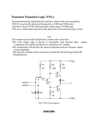
Bipolar Junction Transistors The transistor is a three-layer semiconductor device consisting of either two n- and one p- type layers of material or two p-and one n- type layers of material. The former is called an npn transistor, while the latter is called a pnp transistor So, there are two types of BJT- i) pnp transistor ii) npn transistor By Biswarup Santra // 8927534666
TransistorStructure BJT is bipolar because both holes (+) and electrons (-) will take part inthe current flow through thedevice N-type regions contains free electrons (negativecarriers) P-type regions contains free holes (positivecarriers) 2 types ofBJT NPNtransistor PNPtransistor The transistor regionsare: Emitter (E) sendthe carriersinto the baseregionand thenonto the collector Base (B) acts as control region. It can allow none,some or many carriers to flow Collector (C) collects the carriers By Biswarup Santra // 8927534666
PNP and NPN transistor structure P N P N P N Ic(mA) IC(mA) IB( A) IB( A) IE(mA) IE(mA) Arrow shows the current flows By Biswarup Santra // 8927534666
TransistorConstruction A transistor has three doped regions. For both types, the base is a narrow region sandwiched between the larger collector and emitter regions. The emitter region is heavily doped and its job is to emit carriers into the base. The base region is very thin and lightly doped. Most of the current carriers injected into the base pass on to the collector. The collector region is moderately doped and is the largest of all three regions. By Biswarup Santra // 8927534666
Naming of Transistor Terminals Transistor has three section of doped semiconductor. The section one side is called emitter and the opposite side is called collector . The middle section is called base . Transistor symbol By Biswarup Santra // 8927534666
Naming of Transistor Terminals 1) Emitter: The section of one side that supplies carriers is called emitter. Emitter is always forward biased wr to base so it can supply carrier. For npn transistor emitter supply holes to its junction. For pnp transistor emitter supply electrons to its junction. By Biswarup Santra // 8927534666
Naming of Transistor Terminals 2) Collector: The section on the other side that collects carrier is called collector. The collector is always reversed biased wr to base. For npn transistor collector receives holes to its junction. For pnp transistor collector receives electrons to its junction. By Biswarup Santra // 8927534666
Naming of Transistor Terminals 3) Base: The middle section which forms two pn junction between emitter and collector is called Base. By Biswarup Santra // 8927534666
Some important factors to be remembered The transistor has three region named emitter, base and collector. The Base is much thinner than other region. Emitter is heavily doped so it can inject large amount of carriers into the base. Base is lightly doped so it can pass most of the carrier to the collector. Collector is moderately doped. By Biswarup Santra // 8927534666
Some important factors to be remembered The junction between emitter and base is called emitter- base junction(emitter diode) and junction between base and collector is called collector-base junction(collector diode). The emitter diode is always forward biased and collector diode is reverse biased. The resistance of emitter diode is very small(forward) and resistance of collector diode is high(reverse). By Biswarup Santra // 8927534666
Transistor Operation 1) Working of npn transistor: Forward bias Is applied to emitter- base junction and reverse bias is applied to collector- base junction. The forward bias in the emitter-base junction causes electrons to move toward base. This constitute emitter current, IE By Biswarup Santra // 8927534666
Transistor Operation 1) Working of npn transistor: As this electrons flow toward p-type base, they try to recombine with holes. As base is lightly doped only few electrons recombine with holes within the base. These recombined electrons constitute small base current. The remainder electrons crosses base and constitute collector current. By Biswarup Santra // 8927534666
Transistor Operation 2) Working of pnp transistor: Forward bias is applied to emitter- base junctionand reverse bias is applied to collector- base junction. The forward bias in the emitter-base junction causes holes to move toward base. This constitute emitter current, IE By Biswarup Santra // 8927534666
Transistor Operation 2) Working of pnp transistor: As this holes flow toward n-type base, they try to recombine with electrons. As base is lightly doped only few holes recombine with electrons within the base. These recombined holes constitute small base current. The remainder holes crosses base and constitute collector current. By Biswarup Santra // 8927534666
Transistor Symbol By Biswarup Santra // 8927534666
Transistor Operating Modes Active Mode Base- Emitter junction is forward and Base- Collector junction is reverse biased. Saturation Mode Base- Emitter junction is forward and Base- Collector junction is forward biased. Cut-off Mode Both junctions are reversebiased. By Biswarup Santra // 8927534666