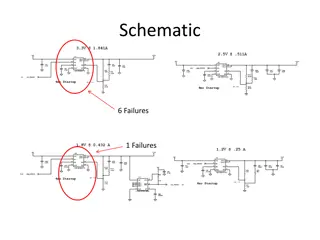
Explore a comprehensive guide for reviewing schematics of CAN and LIN devices before seeking assistance on technical forums. Understand pin functions, placement guidelines, and component requirements for optimal performance. Enhance your understanding of transceiver interfaces and selective disclosure of information.
Please find below an Image/Link to download the presentation.
The content on the website is provided AS IS for your information and personal use only. It may not be sold, licensed, or shared on other websites without obtaining consent from the author. If you encounter any issues during the download, it is possible that the publisher has removed the file from their server.
You are allowed to download the files provided on this website for personal or commercial use, subject to the condition that they are used lawfully. All files are the property of their respective owners.
The content on the website is provided AS IS for your information and personal use only. It may not be sold, licensed, or shared on other websites without obtaining consent from the author.
Introduction This document provides basic schematic review guide for CAN and LIN devices. This document helps users to review schematic and layout by themselves before posting any schematic review thread on E2E. 8-pin package guide works for common pins on 14-pin package. Please refer to datasheet for each pin s more detailed function description. For those digital I/O pins not mentioned here, no external components are needed. Users can connect them directly to MCU. TI Information Selective Disclosure
8-Pin Packages 5V CAN FD Family TCAN1044A(V)-Q1 / TCAN1057A(V)-Q1 TCAN1042H / TCAN1051H-Q1(HG/HGV) 4.9mm 3.0mm 2.9mm CAN SIC Family TCAN1462(V)-Q1 SOIC VSON SOT-8 5.9mm 3.0mm 2.8mm LIN Family TLINx021A-Q1 TLINx029A-Q1 TLIN1039-Q1 TI Information Selective Disclosure
8-pin CAN Transceivers TXD, RXD Series resistors can be placed on these digital lines (not required). Those resistors are more often used to limit the switching current through the signal lines during transitions to limit EMI. Typical values for such resistors will be between 10 and 33 . The TXD pin is internally pulled-up so the pin is in a known state in case it s left floating. If the user chooses to use external pull-up the typical value is 10 k . TI Information Selective Disclosure
VCC, VIO In addition to the power supply filtering, a decoupling capacitance typically 100 nF should be placed near the CAN transceiver's main VCC and VIO supply pins. If VIO is not in use, consider tying this pin to VCC with optional 100 nF placement. STB / S The pin has internal pull-up to avoid pin floats. It is specified to have a maximum low-level leakage current of -20 A when driven to 0V. This would roughly equate to an internal pull-up strength of 275 k . Users can choose to add external pull-down resistor to avoid the negative voltage in GND. If normal mode is the only intended mode of operation, the STB pin can be tied directly to GND. If silent mode is the only intended mode of operation, the S pin can be tied directly to a static system voltage source using a pull-up resistor. TI Information Selective Disclosure
CANH, CANL For CAN termination please refer to Application Information Disclaimer section in datasheets. Bus filtering capacitors are optional, typically 100 nF. Common mode choke is not required, but it is highly recommended to filter common node noise as necessary for harsh EMC environment or if the user has EMC concerns about their designs. For CMC choice please refer to the app note at https://www.ti.com/lit/pdf/slla271 TVS diode is optional but recommended for extra ESD protection. The user should at least have the footprints for the TVS diode on the bus, unless application environment is certainly won't have voltage transients that violate the absolute maximum specification. TI offers ESD2CAN24- Q1 for CAN applications. TI Information Selective Disclosure
8-pin LIN Transceivers RXD If the microprocessor paired with the transceiver does not have an integrated pull-up, an external pull-up resistor in the range of 1 k to 10 k is required to be placed between RXD pin and the supply voltage for the controller. TXD A series resistor can be placed to limit the input current to the device. A capacitor to ground can be placed close to the input pin of the device to filter noise. TI Information Selective Disclosure
EN It has an internal pull-up resistor to avoid left floating so no external pull-up is required. If this feature is not used, it can be connected to the supply voltage for the controller through a series resistor between 1 k and 10 k . Additionally, a series current-limiting resistor may be placed on the pin in the case of an over voltage fault. VSUP A 100 nF decoupling capacitor should be placed as close to the device as possible. WAKE The pin can be used with a switch to VSUP or to ground. A series resistor is needed for protection against over current conditions as it limits the current into the WAKE pin when the ECU has lost its ground connection.A pull-up resistor is required to provide sufficient current during stimulation of a WAKE event. If the terminal is unused it should be pulled to VSUP or ground to avoid unwanted parasitic wake-up events. TI Information Selective Disclosure
INH A 100 k load can be added to the INH output to ensure a fast transition time from the driven high state to the low state and to also force the pin low when left floating. LIN For responder mode applications, a 220 pF capacitor to ground need to be implemented. For commander mode applications, an additional series resistor and blocking diode should be placed between the LIN pin and the VSUP pin. Optional external TVS diode is applicable for extra ESD protection. TI offers ESD1LIN24-Q1 as an option for LIN interface. TI Information Selective Disclosure
14-Pin Packages 5V Multi-channel CAN FD Family TCAN1046A-Q1 TCAN1046AV-Q1 / TCAN1048AV-Q1 5V Wake / INH CAN FD Family TCAN1043A-Q1 TCAN1162x-Q1 CAN SIC Transceiver Family TCAN1043H-Q1 TCAN1463-Q1 5V CAN Partial Networking Family LIN Transceiver Family TCAN114x-Q1 TLINx022A-Q1 TI Information Selective Disclosure
14-pin CAN Transceivers EN, nSTB The pin is internally pulled low to prevent excessive system power and false wake-up events. Users can choose to add 10 K external pull-up resistor for noise immunity or to bias the signal when the transceiver is unpowered but is not required because those inputs already has an internal bias. TI Information Selective Disclosure
INH A 100 k load can be added to the INH output for a fast transition time from the driven high state to the low state and to force the pin low when left floating. INH_MASK The pin can be used to disable and enable the INH function when in Silent mode. It can be left floating or connected to GND if the functionality is not used. A 100 k load can be added for a fast transition time from the driven high state to the low state and to force the pin low when left floating. Wake The pin is usually connected to an external switch. See Application Information Disclaimer or Layout section in datasheets for detail circuit configuration. See Local Wake-Up (LWU) via WAKE Input Terminal section in datasheet when choosing a resistor value for WAKE pin. It will be related to the maximum battery voltage used and the leakage characteristics of the pin. TI Information Selective Disclosure
VFLT The pin requires a 10 F external capacitor as close to the pin as possible. SDO/nINT When working as nINT, an external resistor to VIO with value between 2 k and 10 k is required. TI Information Selective Disclosure
14-pin LIN Transceivers *Please refer to 8-pin LIN transceivers TI Information Selective Disclosure
Layout Tips Please refer to EVM manual and the Layout section in datasheets for more details. Ensure bus filter placed close to connector and along signal path. Ensure TVS diode placed close to connector and along signal path. Ensure CMC placed nominally between transceiver and termination. Avoid CAN lines vias to under-side of board where possible. Keep a common flow of the CAN signal from left-to-right. This would make trace length matching easier. Use at least two vias for supply and ground connections of bypass capacitors and protection devices to minimize trace and via inductance. Power lines routed under the CAN bus is non-ideal. TI Information Selective Disclosure