CANbusRUv1 Block Diagram Fanout Xtal 160MHz Last Update
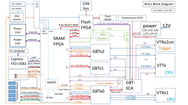
This diagram outlines the components and connections of a CANbusRUv1 system, featuring elements such as a jitter cleaner, flash PROM, temperature monitoring via RTD, various voltage power units, communication interfaces like I2C, FPGA components, and more. The architecture includes a selection of 8-bit mapping, JTAG headers, monitoring for voltage/current, SRAM, and programmable logic devices. The system integrates intricate features such as MGT RefClk, UsrClk, MLVDS, VGA connectors, and ADC for efficient operation and control across different power domains.

Uploaded on Mar 09, 2025 | 2 Views
Download Presentation

Please find below an Image/Link to download the presentation.
The content on the website is provided AS IS for your information and personal use only. It may not be sold, licensed, or shared on other websites without obtaining consent from the author.If you encounter any issues during the download, it is possible that the publisher has removed the file from their server.
You are allowed to download the files provided on this website for personal or commercial use, subject to the condition that they are used lawfully. All files are the property of their respective owners.
The content on the website is provided AS IS for your information and personal use only. It may not be sold, licensed, or shared on other websites without obtaining consent from the author.
E N D
Presentation Transcript
CAN bus RUv1 Block Diagram fan out Xtal 160MHz Xtal 160MHz Last Update: 1-Dec-2017 Jitter cleaner Flash PROM Temperature (RTD) Flash FPGA 2 I2C for monitoring/Control 12V power 3,3V 2,5V 1,8V 1,5V 1,2V 1V 8 bit SELECT MAP Power Unit JTAG 12 DIO 5 DIO 5 DIO MGT RefClk UsrClk 8 MLVDS SCA ADC JTAG Headers En Monitor voltage/current SRAM FPGA Power Unit 8 MLVDS VTRx2sm Trigger I2C 4.8 Gbps 2xclkdes (40, 160MHz) HR Bank 10x320 Mbps Dout Trigger GBTx2 I2C EEPROM 4.8 Gbps 10 x 320 Mbps Din I2C UART Cypress FX3-USB3 I2C 13bit Ctrl PCLK-100MHz VTTx 10 x 320 Mbps Din 4.8 Gbps 32bit Data HR Bank GBTx1 I2C 4 AUX IO CRU Busy out Busy in I2C MGT I2C I2C GBT- SCA switch Clkdes (40Mhz) FireFly Transition Board I2C 2 Clkdes 2 Clkdes 2 UsrClk FireFly 28 Data (1.2Gbps) MGT 2 MGT RefClk GBTx0 VTRx1 FireFly 2xclkdes (40, 160MHz) SCA e-link 28 Data (400/600M) I2C 160 MHz LVDS 10 x 320 Mbps Din 5 DCLK (MLVDS) 5 DCTRL (MLVDS) FireFly 4.8 Gbps 40 MHz LVDS HR Bank 10 x 320 Mbps Dout CRU 4.8 Gbps FireFly LVDS 1 Clkdes
MFT connections: MFT connections: For the two smallest disks, MFT needs to read sensors at 1.2 RU, split into 3 ladders 3 ladders, therefore 3 3 clk On the larger disks, switching to 600 into 5 5 ladders ladders, so 5 5 clk clk/ctrl/data cable assemblies /ctrl/data cable assemblies are required. 1.2 Gb/s Gb/s, at most there are 11 11 ALPIDEs ALPIDEs connected to a single clk/ctrl/data cable assemblies /ctrl/data cable assemblies are required. 600 Mb/s Mb/s readout is possible. There are at most 21 ALPIDE 21 ALPIDE connected to a single RU split A A B B C C D D E E used unused Connector Connector 1.2 Gb/s 400 or 600 Mb/s Unconnected ITS IL ITS IL ITS ML/OL ITS ML/OL MFT ID MFT ID MFT OD MFT OD Would require specific lowlevel firmware for the MFT
Possible SRAM FPGA choices: UltraScale & UltraScale+ pin-to-pin compatible devices in A1156 package (35 35 mm2). Only need to check maximum voltage range for some HR banks between US/US+. We will likely need 250 (ITS) + 100 (MFT) FPGAs (including spares). Current
General Specifications 1 ALICE ITS UPGRADE High Speed I/Os 400/600 Mbps readout of sensors via LVDS has not yet been tested. Matthias has created the firmware necessary to test it, but actual hardware test has not yet been done. Need to check the compatibility for SLVS and MLVS in the various banks and number of inputs needed with these voltages Need to check the number of links for both ITS and MFT GBT GBTx 1 and 3 get their clocks from downlink (CRU & CTP respectively). GBTx 2 gets is clock from GBTx 1 via clkdes line Bring 3 clkdes into SRAM FPGA: 160MHz, 40 MHz (Serdes clock), 320MHz (?, elink speed) JTAG is provided via SCA to both SRAM and Flash FPGA in JTAG chain with jumpers to isolate each part. Add local headers for both SRAM and Flash FPGA Flash FPGA can communicate with CRU via I2C Busy Busy in and out channels via MGT need to be provided to investigate busy handling schemes
General Specifications 2 ALICE ITS UPGRADE Radiation Hardness Choice of Flash FPGA still open. ProAsic3 is preferred choice, but it is rumored it has reprogrammability issues similar to IGLOO2. Flash FPGA uses SelectMap interface to program SRAM FPGA at power-up. It also uses SelectMap interface for scrubbing. For both purposes, the images are stored in the FlashProm attached to the Flash FPGA (different images?). Two I2C buses through the GBT-SCA are used for control and monitoring communication with the CRU During shutdowns when GBT isn t available, a CANbus interface is used for control & monitoring of PowerUnit. CANbus lines can also be forwarded (via Firmware) from FlashFPGA to SRAM-FPGA to run CANbus core there instead. SRAM-FPGA is responsible for interaction with PU (control, monitoring, latchup-response). Needs to communicate PU status (including latchup) to FlashFPGA for monitoring via GBT (or CANbus) For reprogramming the FlashPROM a special firmware could be loaded to SRAM-FPGA to provide data path from GBT through communication bus to FlashFPGA (and in turn to PROM). Mechanics Single-sided component mounting
SRAM FPGA IO resources needed ALICE ITS UPGRADE For each GBT DP 10 DP 10 at 320 Mb/s e-links (160 MHz). FX3 chipset DP 1 DP 1 at 160 MHz clock e-link. SE 1 SE 1 UART. DP 1 DP 1 at 40 MHz clock e-link. SE 1 SE 1 Clock. DP 12 DP 12 IO pairs for each GBTx. SE 14 SE 14 bit control. In total (5 GBT links through 3 GBTx chip), data communication only. SE 32 SE 32 Bit data. DP DP 60 60 toward the GBTx. SE 48 SE 48 total. Flash FPGA connection Power Unit SE 32 SE 32 select MAP. SE 2 SE 2 3 3 line (HS I2C ) for (2 power unit). SE 32 SE 32 data/control. SE 2 SE 2 16 16 line (8 analog + 8 digital LU/SEU monitor). SE SE 64 64 total.