Capacitance and Resistance Analysis for Frequency Response in Amplifiers
Explore the frequency response of amplifiers through capacitance and resistance analysis for poles and zeros. Learn how to determine capacitance, resistance, gain characteristics, and frequency roll-off in different frequency bands. Understand the impact of coupling and bypass capacitors on the low-frequency response and how to determine the lower 3dB frequency in amplifier circuits.

Download Presentation

Please find below an Image/Link to download the presentation.
The content on the website is provided AS IS for your information and personal use only. It may not be sold, licensed, or shared on other websites without obtaining consent from the author. If you encounter any issues during the download, it is possible that the publisher has removed the file from their server.
You are allowed to download the files provided on this website for personal or commercial use, subject to the condition that they are used lawfully. All files are the property of their respective owners.
The content on the website is provided AS IS for your information and personal use only. It may not be sold, licensed, or shared on other websites without obtaining consent from the author.
E N D
Presentation Transcript
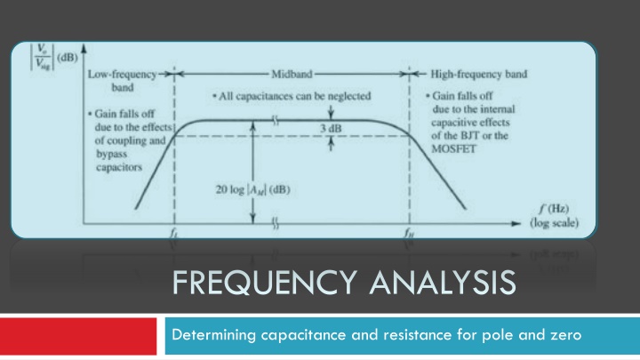
FREQUENCY ANALYSIS Determining capacitance and resistance for pole and zero
Frequency Response of Amplifiers Midband: The frequency range of interest for amplifiers Large capacitors can be treated as short circuit and small capacitors can be treated as open circuit Gain is constant and can be obtained by small- signal analysis
Frequency Response of Amplifiers Low-frequency band: Gain drops at frequencies lower than fL Large capacitors can no longer be treated as short circuit The gain roll-off is mainly due to coupling and by-pass capacitors
Frequency Response of Amplifiers High-frequency band: Gain drops at frequencies higher than fH Small capacitors can no longer treated as open circuit The gain roll-off is mainly due to parasitic capacitances of the MOSFETs
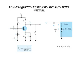
Low Frequency Response for Common Source Amplifiers Small Signal Analysis ( ) V || g R R + R s s s g m G D R L = + + + V R s s s 1 2 3 sig G sig p p p First pole derivation R 1 G = V V g sig Where + + R R G sig sC 1 C 1 = ( ) R + s 1 p G = + V C R R sig 1 1 C G sig R R + ( ) s G sig + C R R 1 C G sig
Low Frequency Response for Common Source Amplifiers Second Pole Derivation (KCL) Small signal Analysis Diagram
Low Frequency Response for Common Source Amplifiers Third Pole derivation = V I R o o L R D 1 = I R d L + + R R D L sC 2 C R R + s D L R = I d 1 R + s D L ( ) + sC R R 2 C D L 1 = ( ) 3 p + C R R 2 C D L
Determining Lower 3dB Frequency Coupling and by-pass capacitors result in a high- pass frequency response with three poles If the poles are sufficiently separated Bode plot can be used to evaluate the response for simplicity The lower 3-dB frequency is the highest-frequency pole P2is typically the highest-frequency pole due to small resistance of 1/gm If the poles are located closely The lower 3-dB frequency has to be evaluated by the transfer function which is more complicated.
Determining the pole frequency by inspection Reduce Vsigto zero Consider each capacitor separately (treat the other capacitors as short circuit) Find the total resistance between the terminals
Selecting values for the coupling and by- pass capacitors These capacitors are typically required for discrete amplifier designs CSis first determined to satisfy needed fL CC1and CC2are chosen such that poles are 5 to 10 times lower than fL
Internal Capacitive Effects and the High-Frequency Model Parasitic Capacitances in the MOSFETs transistor
Capacitance in the MOSFET There are basically two types of internal capacitance in the MOSFET Gate capacitance effect: the gate electrode forms a parallel-plate capacitor with gate oxide in the middle Junction capacitance effect: the source/body and drain/body are pn-junctions at reverse bias The gate capacitive effects
Gate capacitance effect 1 MOSFET in triode region: = = + C C WLC C gs gd OX ov 2 2 MOSFET in saturation region: =3 + = C WLC C C C gs OX ov gd ov MOSFET in cutoff region: = = C C C gs gd ov 1 = C WLC gb OX 2
Cov is the Overlap Capacitance Overlap capacitance: = C WL C ov ov ox L overlap is the length of the drain/source under the gate
Junction Capacitance Junction capacitance includes components from the bottom side and from the side walls The simplified expression are given by: C C 0 0 sb V db V = = C C sb db + + 1 1 SB SB V V o o
MOSFET High Frequency Model Simplified high-frequency MOSFET model Source and body terminals are shorted Cgd plays an important role in the amplifier frequency response Cdb is neglected to simplify the analysis W ( ) = 2 g C V V m n ox GS t L = g g | mb m | V A = r o I d
Unity Gain Frequency The frequency at which the current gain becomes unity fTIs typically used as an indicator to evaluate the high-frequency capability Smaller parasitic capacitances Cgsand Cgdare desirable for higher unity-gain frequency
Analysis for unity frequency The unity-gain frequency is strongly influenced by the channel length Higher unity-gain frequency can be achieved for a given MOSFET by increasing the bias current or the overdrive voltage The unity-gain frequency can also be expressed as
Common Source Amplifier Midband gain: R + ( ) G = A g R M m L R R G sig Frequency response V V = V ( ) sig gs gs + + sC V sC V V gs gd gs o R R sig G ( ) V o = + sC V V g V gd gs o m gs ' L R
Common Source Amplifier The common-source amplifier has one zero and two poles at higher frequencies The amplifier gain falls off at frequencies beyond midband The amplifier bandwidth is defined by the 3-dB frequency which is typically evaluated by the dominant pole (the lowest-frequency pole) in the transfer function
Simplified Analysis Technique Assuming the gain is nearly constant ( -gmR L) Find the equivalent capacitance of Cgdat the input (with identical Igd) This is the Miller effect
Simplified Analysis Technique Neglect the small current Igdat the output The dominant pole is normally determined by Ceq The frequency response of the common- source amplifier is approximated by a STC
Widescreen Test Pattern (16:9) Aspect Ratio Test (Should appear circular) 4x3 16x9


")