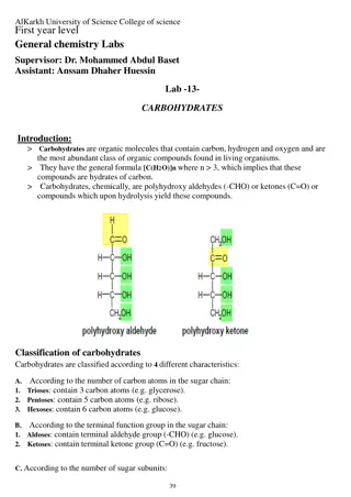
Carbohydrates: Definition and Chemical Structure Overview

Carbohydrates are essential compounds in cell function, classified into monosaccharides, oligosaccharides, and polysaccharides based on structure and properties. They exhibit optical activity and can be aldoses or ketoses. Learn more about their classification and characteristics in this comprehensive guide.

Download Presentation

Please find below an Image/Link to download the presentation.
The content on the website is provided AS IS for your information and personal use only. It may not be sold, licensed, or shared on other websites without obtaining consent from the author.If you encounter any issues during the download, it is possible that the publisher has removed the file from their server.
You are allowed to download the files provided on this website for personal or commercial use, subject to the condition that they are used lawfully. All files are the property of their respective owners.
The content on the website is provided AS IS for your information and personal use only. It may not be sold, licensed, or shared on other websites without obtaining consent from the author.
E N D
Presentation Transcript
CEPC APDR Study Zhenchao LIU 2016-11-4
Problems in PDR The peak power of bunch train is very high(several MW), however, there is no such large power input coupler. Power compensation will cause low RF efficiency. No power compensation will cause RF voltage drop and phase shift. Power coupler limit. e.g. Accelerator gradient decrease in one RF cavity (H-high lumi.)(The peak beam power is 4.9MW@15MV/m; Assume 300kW input power & 15MV/m of the 5cell cavity Final Eacc/Initial Eacc Final Eacc/Initial Eacc RF cycles Initial Eacc(MV/m) Field decrease in one cavity at the bunch train passing period The design is very challenging for the RF! Field decrease vs. various initial field gradient of the cavity
Limitations on the power coupler The average power of input coupler is ~300kW The peak power of input coupler is ~1MW . The maximum power is limited by the ceramic window S. Belomestnykh OVERVIEW OF INPUT POWER COUPLER DEVELOPMENTS PULSED AND CW WE305, SRF2007
Nonconstant Voltage and Phase (NVP) Acceleration method New acceleration method for CEPC to solve RF efficiency The bunches in a bunch train will be accelerated at different Vci The bunches in a bunch train will be accelerated at different synchrotron phase to keep constant energy gain. Vai=Vci*cos si=C
parameter for CEPC partial double ring wangdou20160325 Pre-CDR H-high lumi. H-low power W Z Number of IPs Energy (GeV) Circumference (km) SR loss/turn (GeV) Half crossing angle (mrad) Piwinski angle Ne/bunch (1011) Bunch number Beam current (mA) SR power /beam (MW) Bending radius (km) Momentum compaction (10-5) IPx/y (m) Emittance x/y (nm) Transverse IP(um) x/IP y/IP VRF(GV) fRF(MHz) Nature z(mm) Total z(mm) HOM power/cavity (kw) Energy spread (%) Energy acceptance (%) Energy acceptance by RF (%) n Life time due to beamstrahlung_cal (minute) F (hour glass) Lmax/IP (1034cm-2s-1) 2 2 2 2 2 120 54 3.1 0 0 3.79 50 16.6 51.7 6.1 3.4 120 54 2.96 15 2.5 2.85 67 16.9 50 6.2 2.5 120 54 2.96 15 2.6 2.67 44 10.5 31.2 6.2 2.2 80 54 0.59 15 5 0.74 400 26.2 15.6 6.1 2.4 45.5 54 0.062 15 7.6 0.46 1100 45.4 2.8 6.1 3.5 0.1/0.001 0.62/0.0028 7.9/0.053 0.006 0.073 0.12 650 3.9 4.0 0.99 0.05 0.8/0.0012 6.12/0.018 69.97/0.15 0.118 0.083 6.87 650 2.14 2.65 3.6 0.13 2 6 0.23 47 0.25/0.00136 2.45/0.0074 24.8/0.1 0.03 0.11 3.62 650 3.1 4.1 2.2 0.13 2 2.2 0.47 36 0.268 /0.00124 2.06 /0.0062 23.5/0.088 0.032 0.11 3.53 650 3.0 4.0 1.3 0.13 2 2.1 0.47 32 0.1/0.001 1.02/0.003 10.1/0.056 0.008 0.074 0.81 650 3.25 3.35 0.99 0.09 1.7 0.3 1.1 0.24 0.68 2.04 0.82 2.96 0.81 2.01 0.92 3.09 0.95 3.09 6
New SRF layout-6 ring IP1 RF station Double Ring (1km/3km) C 60km RF&DR center 30 equispaced IP3
6 double ring APDR (H-low power) 2 120 54 2.96 15 2.6 2.67 15x3 10.5 31.2 6.2 3.53 650 384 20 33-30.9 163 1148 62.7 2 8 8 48 206 268 0.54 0.485 2 2E10 1.242 2.536e6 0.128 -0.083 100 5.484 26.7 ~100 2.2 0.021 APDR(HL VRF=3.62) APDR (Z) Number of IPs Energy (GeV) Circumference (km) SR loss/turn (GeV) Half crossing angle (mrad) Piwinski angle Ne/bunch (1011) Bunch number Beam current (mA) SR power /beam (MW) Bending radius (km) VRF(GV) fRF(MHz) Cavity No. Cavity gradient Accelerating phase CW power/cavity kW Peak power/train (kW) Total Power MW) Cell/cavity Cavity/module Module/station Total module R/Q ( ) G HOM loss factor/cavity (V/pC) HOM power/cavity (kW) Working Temperature K Q0 ms QL Bandwidth(kHz) Detuning F (kHz) Stored energy/cavity(J) Frev(kHz) Gap length (us) (RF to beam efficiency)(%) Vc decrease(%) TB/ 2 2 120 54 2.96 15 2.5 2.85 22x3 17 50 6.2 3.62 650 384 20.6 35.2-32.3 260 2345 100.4 2 8 8 48 206 268 0.54 0.838 2 2E10 0.811 1.656e6 0.196 -0.138 107.4 5.484 26.7 ~100 3.3 0.0158 45.5 54 0.062 15 8.5 0.46 367x3 45.4 2.8 6.1 0.357/0/12 650 48/24 16.2/21.7 80.2-79.8/58.9-56.9 117/233 1237 5.6 2/1 4/4 2/1 12/6 206/103 268 0.54 0.361/0.18 2 2E10 2.243/0.507 4.58e6/1.03e6 0.071/0.314 -0.234/-0.520 65.3/59.1 5.484 26.7 ~100 2.5/5.3 0.012/0.053
Accelerator gradient decrease in one RF cavity (Z) Bunch train passing Bunch train space Assume matching Final Eacc/Initial Eacc Final Eacc/Initial Eacc Initial Eacc(MV/m) RF cycles Field evolution in cavity Field decrease vs. various initial field gradient of the cavity
New SRF layout-8 ring IP1 RF station Double Ring (1km/3km) C 62km RF&DR center 22.5 equispaced IP3
8 double ring APDR(HL VRF=3.62) APDR (H-low power VRF=3.53) APDR (Z) Number of IPs Energy (GeV) Circumference (km) SR loss/turn (GeV) Half crossing angle (mrad) Piwinski angle Ne/bunch (1011) Bunch number Beam current (mA) SR power /beam (MW) Bending radius (km) VRF(GV) fRF(MHz) Cavity No. Cavity gradient 2 2 2 120 54 2.96 15 2.5 2.85 17x4 17 50 6.2 3.62 650 384 20.6 35.2-33 120 54 2.96 15 2.6 2.67 11x4 10.5 31.2 6.2 3.53 650 45.5 54 0.062 15 8.5 0.46 275x4 45.4 2.8 6.1 0.357/0.12/0.12 650 48/16/16 16.2/16.3/32.6 80.1-79.9/58.9-56.9/58.9-58 384/768/192 20/20/20 33-31.6/33-31.6/33-31.6 Accelerating phase 260 1389 100.4 2 6 8 64 206 268 0.54 0.838 2 2E10 0.811 1.656e6 0.196 -0.138 107.4 5.484 20 ~100 2.5 0.025 163.3/81.6/326.6 843 62.7 2/1/4 6/12/3 8/8/8 64/64/64 206/103/412 268 0.54/0.27/1.08 0.485/0.24/0.97 2 2E10 1.242 2.53e6 0.128 -0.083 100 5.484 20 ~100 1.6 0.0098 117/350/350 884 5.6 2/2/1 6/2/2 1/1/1 8/8/8 206/206/103 268 0.54/0.54/0.27 0.36/0.36/0.18 2 2E10 2.243/0.76/0.76 4.58e6/1.55e6/1.55e6 0.071/0.209/0.209 -0.234/-0.347/-0.347 65.3/65.3/133 5.484 20 ~100 1.7/5.3/2.5 0.0089/0.0263/0.0263 CW power/cavity kW Peak power/train (kW) Total Power MW Cell/cavity Cavity/module Module/station Total module R/Q ( ) G HOM loss factor/cavity (V/pC) HOM power/cavity (kW) Working Temperature K Q0 ms QL Bandwidth(kHz) Detuning F (kHz) Stored energy/cavity(J) Frev(kHz) Gap length TB (us) (RF to beam efficiency)(%) Vc decrease(%) TB/
Phase shift Pcw<<Ppulsecase: Larger synchrotron phase will make smaller phase shift for the bunches in a bunch train for the same voltage drop Large voltage drop should choose larger synchrotron phase Large synchrotron phase means more cavities (more cost) Phase shift (degree) APDR case 2% Vc decrease 4% Vc decrease PDR case 10% Vc decrease 20% Vc decrease Synchrotron phase of first bunch (degree)
Bunch No. Pre CDR (CW, Pg=Pavg) PDR (CW, Pg=Ppulse, very low RF efficiency) APDR 8 ring (HL, CW, Pg=Pavg) APDR 8 ring (H- low power, CW, Pg=Pavg) APDR 8 ring (Z, Pg=Pavg) Vc Phase shift Vc Phase shift Vc Phase shift Vc Phase shift Vc Phase shift 1 2.00 1 1.40 1 2.0000 1 1 0 1 0 0.9984 1.88 0.9984 1.26 0.9998 1.9927 2 1 0 1 0 0.9969 1.75 0.9968 1.12 0.9996 1.9855 3 1 0 1 0 0.9953 1.63 0.9952 0.98 0.9994 1.9782 4 1 0 1 0 0.9938 1.50 0.9936 0.84 0.9992 1.9709 5 1 0 1 0 0.9922 1.38 0.992 0.70 0.9990 1.9636 6 1 0 1 0 0.9906 1.25 0.9904 0.56 0.9988 1.9564 7 1 0 1 0 0.9891 1.13 0.9888 0.42 0.9987 1.9491 8 1 0 1 0 0.9875 1.00 0.9872 0.28 0.9985 1.9418 9 1 0 1 0 0.9859 0.88 0.9856 0.14 0.9983 1.9345 10 1 0 1 0 0.9844 0.75 0.984 0 0.9981 1.9273 11 1 0 1 0 0.9781 0.25 0.9973 1.8982 1 0 1 0 15 0.9750 0.9969 1.8836 1 0 1 0 0 17 0.9906 1.6436 1 0 1 0 50 0.9873 1.5200 1 0 67 0.0947 0 275 Assume Vrfis constant at the first bunch of bunch trains and the change of Vbis negligible.
Bunch No. Pre CDR (CW, Pg=Pavg) PDR (CW, Pg=Ppulse, very low RF efficiency) APDR 6 ring (H- low power, CW, Pg=Pavg) APDR 6 ring (HL, CW, Pg=Pavg) APDR 6 ring (Z, Pg=Pavg) Vc Phase shift Vc Phase shift Vc Phase shift Vc Phase shift Vc Phase shift 1 2.20 1 2.60 1 2.6000 1 1 0 1 0 0.9984 2.04 0.9984 2.48 0.9998 2.5929 2 1 0 1 0 0.9968 1.89 0.9969 2.35 0.9996 2.5858 3 1 0 1 0 0.9952 1.73 0.9953 2.23 0.9994 2.5787 4 1 0 1 0 0.9936 1.57 0.9937 2.10 0.9992 2.5716 5 1 0 1 0 0.992 1.41 0.9921 1.98 0.9989 2.5645 6 1 0 1 0 0.9904 1.26 0.9906 1.86 0.9987 2.5574 7 1 0 1 0 0.9888 1.10 0.9890 1.73 0.9985 2.5503 8 1 0 1 0 0.9872 0.94 0.9874 1.61 0.9983 2.5432 9 1 0 1 0 0.9856 0.79 0.9859 1.49 0.9981 2.5361 10 1 0 1 0 0.984 0.63 0.9843 1.36 0.9979 2.5290 11 1 0 1 0 0.9776 0 0.9780 0.87 0.9971 2.5005 1 0 1 0 15 0.9670 0.9956 2.4508 1 0 1 0 0 22 0.9897 2.2519 1 0 1 0 50 0.9861 2.1311 1 0 67 0.0923 0 367 Assume Vrfis constant at the first bunch of bunch trains and the change of Vbis negligible.
Compare with LEP Assume: e= 1deg., s=116deg., align=3deg., Ib=0.45mA, h=31324, Q=40000, Rs=774M 14 cavities V0(initial peak voltage)from 20MV-100MV 2.3MV/cavity(acc. voltage) Voltage decrease: Vleft/V0 1 bunch ~1% 4 bunches ~4% APDR: 8 DR: 2.5%(HL)5.3/2.5%(Z) 6 DR: 3.3%(HL) V0(V) Voltage drop is acceptable!
Bunch position The e+ and e- bunch trains should be symmetry to the two IPs. The phase shift of the synchrotron phase between each bunch in a bunch train is 0.14 degree for the H low power mode. The total phase shift is 1.4 degree. After enough synchrotron damping, the bunches will be at its synchrotron phase separately. If the transport matrix from cavity to IP is the same for e+ and e- bunch trains, there will be no shift for the position of colliding. RADIATION DAMPING, R.P. Walker
Cavity requirements Aim: To minimize the RF voltage drop of the cavity Solutions: Voltage drop formula: R/Q=Vc^2/ U, assume Ppulse>>Pcw c V ( ) ( / ) V dN q R Q N = 1 SR cav b (by Z.C. Liu) 2 V ( ) V N c RF cav d, cavity effective length, q bunch charge, Nbbunches per train, Ncavcavity number. Proper RF cavity number Proper RF cavity gradient Proper RF cavity R/Q for the large voltage drop cavities
Conclusion The 8-double ring and 6-double ring are available when using the same parameter as PDR(VRF=3.62GV) for HL. The 8-double ring has a lower phase variation than the 6-double ring . The phase region is from 35.2-33 degree for bunches in a bunch train for the 8-double ring HL mode. The phase region is from 35.2- 32.3 degree for the 6-double ring HL mode. The bunch energy gain in each cavity is constant. The RF to beam efficiency is ~100%. Vbreaches constant value after about 65 circles (Ib=C, ~0.012s). Beam can be stored by increasing bunch charges stably (with reflection in low current). Vcshould keep constant phase and value for each bunch separately.
RF compensation Aim : To compensate the voltage drop. Solutions: DF cavity? Keep voltage constant RF induce no higher order perturbation + = cos cos nqV mqV C i i di di n, total cavity number; q, bunch charge; Vi, cavity voltage when the ithbunch passed; i, RF phase of the ithbunch in cavity; m, total DF cavity number; Vdi, DF cavity voltage when the ithbunch passed; di, RF phase of the ithbunch in DF cavity. Assume each bunch has a constant phase iin the cavity and diin the DF cavity.
Simple case Assume there are two bunches First order of energy gain: Energy gain: + = sin sin nqV mqV C + = cos V cos nqV mqV C i i di di i i di di V = assume sin n 0 mV V 1 d di d ( sin sin ) V ( cos cos ) n V V = sin 1 1 2 2 = cos - cos 1 1 2 2 2 d 2 1 d d mV 2 d d sin sin 0 if V V cos cos 0 & if V V V V 1 1 2 2 1 1 2 2 1 2 0 sin d 1 - 0 cos - cos 2 2 d 2 1 d d = 0 & 0 0 or 0 2 1 d 2 1 1 2 d d d d = 0 2 1 d d ( sin sin ) n V V = arc sin[ ] 1 1 2 2 2 d mV 2 d
Problems DF cavity should be proper located to fix the bunch position at equal space at IP or RF cavity. Asymmetry is needed in the two rings. Lattice simulation with two types of cavity is needed.


")