CMOS Common Source Amplifier Region III Voltage Transfer Characteristics
An analysis of a CMOS common source amplifier operating in Region III, the high gain region. Details on saturation regions for transistors Q1 and Q2, voltage transfer characteristics, and intersection of I-V curves. Includes solutions and small signal parameters. Neglects channel-length modulation in DC analyses.

Download Presentation

Please find below an Image/Link to download the presentation.
The content on the website is provided AS IS for your information and personal use only. It may not be sold, licensed, or shared on other websites without obtaining consent from the author. If you encounter any issues during the download, it is possible that the publisher has removed the file from their server.
You are allowed to download the files provided on this website for personal or commercial use, subject to the condition that they are used lawfully. All files are the property of their respective owners.
The content on the website is provided AS IS for your information and personal use only. It may not be sold, licensed, or shared on other websites without obtaining consent from the author.
E N D
Presentation Transcript
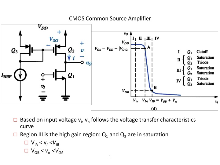
CMOS Common Source Amplifier Based on input voltage vI, vo follows the voltage transfer characteristics curve Region III is the high gain region: Q1 and Q2 are in saturation VIA < vI <VIB VOB < vo <VOA 1
Q2 saturation I-V (Q2) i (2) v=|Vov2| (1) v=0 v Q2 saturation i Function of v, Function of vo v = VDD vo Q2 sat: vo < VDD-|VOV2| (1) vo=VDD (2) vo=VDD-|Vov2| vo 2 EECE 311 - Introduction
I-V (Q1) i Q1 saturation Increasing vi vo I-V of Q1 Function of vo, EECE 311 - Introduction3
Q1 & Q2 (i vs. vo) Q1 saturation i vo Q2 saturation i Intersection of I-V(Q1) I-V(Q2) provides the solution space (1) vo=VDD (2) vo=VDD-|Vov2| vo 4 EECE 311 - Introduction
Q1 & Q2 (i vs. vo) Q1 saturation i Q2 saturation (1) vo=VDD (3) vo=Vov1 (2) vo=VDD-|Vov2| VOA vo VOB Q1 sat: vo >|VOV1| Q2 sat: vo < VDD-|VOV2| 5 EECE 311 - Introduction
Q1 & Q2 (i vs. vo) Q1 saturation i Q2 saturation (1) vo=VDD (3) vo=Vov1 VOB (2) vo=VDD-|Vov2| VOA vo vOA= VDD-|VOV2|=VDD-(VSG-|vtp|) can be derived from IQ3=Iref by solving for VSG vOB can be solved by equating: iQ2 =iQ1 @ vo=vov1 iQ2= 1 iQ1= 1 2?? ? 2?? ? ?(??? |???|)2(1 +??? ???1 ?(???1)2(1 +???1 ) ?? ??) EECE 311 - Introduction6
= = = = 100 A I I I Solution: 1 2 D D REF = = 200 (10) ' 2 2 100 A = I k V V W L 1 2 1 2 1 1 1 D n OV OV 0.316V V 1 OV 100 I V = = = 0.633 mA/V 1 g D 1 m 0.5 0.316V 20 200K 100 1 2 1 OV V I = = = An r 1 o 1 D V 10 Ap = = = 100K r 2 o 100 I 2 D Output resistance: // Voltage gain: A g = We will neglect channel- length modulation in DC analyses. (i.e., when we solve for ID, VOV) = = 66.67K R r r 1 2 o o o ( ) = // 42.2 V/V r r 1 1 2 v m o o When we solve for small signal parameters we will consider those effects Limits of output voltage swing: ( ) 2 ( ) 2 = = = 65 (10) ' p 100 A 0.6 I k V V V W L 1 2 1 2 REF SG tp SG = = = 1.155V 1.155 0.6 0.555V V V 2 SG OV enters SAT when: V V = Q v Q v 2 3 0.555 = = 2.445 V 2 O DD OV enters SAT when: 0.316 V OV V = = 1 7 1 O


")
")
")
")