CMOS Two-Stage Op-Amp Design Constraints and Sizing Process
Explore the design constraints, degrees of freedom, and sizing process involved in creating a CMOS two-stage op-amp. Understand the importance of equality and inequality constraints, along with automated sizing algorithms. Discover how to navigate the complex optimization challenges in op-amp design.

Uploaded on | 4 Views
Download Presentation

Please find below an Image/Link to download the presentation.
The content on the website is provided AS IS for your information and personal use only. It may not be sold, licensed, or shared on other websites without obtaining consent from the author. If you encounter any issues during the download, it is possible that the publisher has removed the file from their server.
You are allowed to download the files provided on this website for personal or commercial use, subject to the condition that they are used lawfully. All files are the property of their respective owners.
The content on the website is provided AS IS for your information and personal use only. It may not be sold, licensed, or shared on other websites without obtaining consent from the author.
E N D
Presentation Transcript
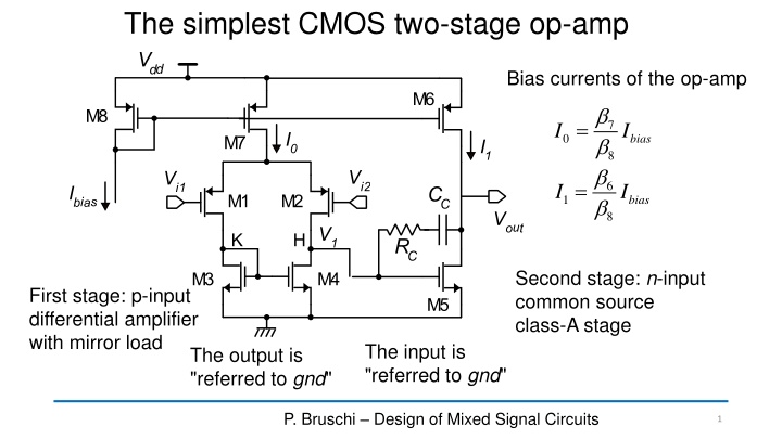
The simplest CMOS two-stage op-amp Bias currents of the op-amp = 7 I I 0 bias 8 = 6 I I 1 bias 8 Second stage: n-input common source class-A stage First stage: p-input differential amplifier with mirror load The input is "referred to gnd" The output is "referred to gnd" P. Bruschi Design of Mixed Signal Circuits 1
Use of a single M8 device to bias multiple op-amp M8 can be shared among different amplifiers and is not part of the op-amp architecture P. Bruschi Microelectronic System Design 2
Degrees Of Freedom (DOFs) Possible DOFs: W, L of all devices (14 DOFs) I0, I1 CC, RC Total: 18 Not all DOFs are independent. It is necessary to choose a set of independent DOFs P. Bruschi Microelectronic System Design 3
Constraints Constraints are relationships among DOFs Two types of constraints: Equality constraints: I I Inequality constraints: = E.g. 6 1 0 7 ( ) GBW DOFs GBW E.g. min P. Bruschi Microelectronic System Design 4
Constraints Every equality constraint reduces the dimension of the DOF space. Equality constraints represent exact conditions that has to be fulfilled in order to guarantee correct operation of the circuit. Some equality constraints derive from simple considerations, such as symmetry: M1=M2, M3=M4. With a few exceptions, equality constraints are specific of the topology and does not depend on the specifications Inequality constraints are derived from the circuit specifications. They does not reduce the dimension of the DOF space but select regions of the DOF space where the specs are met. P. Bruschi Microelectronic System Design 5
The sizing process Combining the various inequality constraints, we find a domain (the intersection of all regions) where all points satisfy all constraints. All points in the domain are valid solutions. If such region does not exist (null intersection), the sizing problem is: "unfeasible". P. Bruschi Microelectronic System Design 6
The sizing process: automatic algorithms Computer programs that perform automatic sizing, are not compatible with an infinite number of feasible solutions. To find a single solution, an optimization condition is often added. If the design is performed manually, any point (set of DOFs values) in the intersection domain is a good solution. Optimization or arbitrary techniques can be used to operate the choice P. Bruschi Microelectronic System Design 7
Sizing of a new topology: steps 1. Find equality constraints to reduce the number of independent DOFs. These constraints will be of two types: (a) Strictly necessary constraints (if not respected the circuit does not work properly) (b) Arbitrary constraints: they are added to further reduce the DOF set and simplify the design. These constraints should be motivated. 2. Choose a set of DOFs that have the following properties: (a) the remaining dependent DOFs can be easily derived from this set; (b) the specifications (inequality constraints) can be written easily and in a simple form as a function of the selected DOFs 3. Write the specifications in terms of the selected DOFs and try to find general design rules. P. Bruschi Microelectronic System Design 8
Equality constraints for the simple 2-stage op-amp Symmetry (necessary to obtain low offset and low CMRR N. of equality constraints M1=M2 (W1=W2, L1=L2) ------ 2 M3=M4 (W3=W4, L3=L4) ------ 2 Current ratios I I / / W W L L = = 6 6 6 1 -------------- 1 0 7 7 7 Initial DOF number: 18 , Resulting DOFs after reduction: 18-5=13 P. Bruschi Microelectronic System Design 9
Necessary constraint: null systematic offset It is not possible to exactly predict Vout, but it will be far from Vdd/ 2 if ISCis consistently different from zero P. Bruschi Microelectronic System Design 10
Necessary constraint: null systematic offset = 6 D I I = = 0 I I I 6 0 6 5 SC D D 7 Since only a common mode voltage is applied to the input: = = V V V V 5 3 H K GS GS I = = 0 I I 3 4 D D 2 I = 0 5 I I 5 D 1 2 2 = 0 5 6 = I 5 6 = 3 I I 0 2 5 6 D D 3 7 3 7 P. Bruschi Microelectronic System Design 11
More constraints 1 2 = 5 6 Null (small) systematic offset 3 7 Arbitrary constraints Good matching M5-M3: L5=L3 Good matching M6-M7: L6=L7 V V Symmetric output swing (same margins to Vdd and gnd) )5 GS t V V GS t 6 ( )5 V V ( = V V GS t GS t 6 P. Bruschi Microelectronic System Design 12
Residual number of DOFs 13 - 4 = 9 Of these residual DOFs we can separate two ones (CCand RC) that do not affect the dc performances and the operating point. We will come back to them later. Then we will focus on 7 DOFs (bias current I0and device size) that affect the operating point and we will call them "static" DOFs). We could select 7 DOFs within the original set (16 DOFs, RC and CC are not included) and then try to derive the remaining ones using the equations that tie them (equality constraints). It is more useful to choose a set of DOFs that may not necessarily include the original 18, in a way that the other ones can be easily derived. P. Bruschi Microelectronic System Design 13
Selection of the 7 DOFs Rationale: the most important MOSFETs of the circuits are M1 (=M2) and M5, since these are the devices that are at the heart of the two stages and that perform the V-to-I conversion. We include all possible DOFs of M1 and M5 into the selected set M1: , , W L V V 1 1 GS V t 6 DOFs 1 M5: , , ( ) W L V 5 5 5 GS t To complete the set, let us include also L6 into the DOSs Final set of static DOFs: 1 1 , , GS W L V , , , ( ) , V W L V V L 5 5 5 6 t GS t 1 P. Bruschi Microelectronic System Design 14
Derivation of all the op-amp parameters from the 7 DOFs All conditions will refer to the operating point (Vid=0) M2 is dentical to M1, then M1 DOFs specify also M2 parameters 0 1 1 5 2 , D D I I I = = = = I C W L ( ) 2 p OX ( , , ) I f W L V V 1 V V 1 1 1 D p GS t GS t 1 1 2 1 W L C ( ) ( ) 2 W L = = , , 5 n OX I f V V V V 5 5 5 D n GS t GS t 5 5 2 = 5 M3=M4: L L 3 5 = D I ( V I 2 C W L I W L 3 1 D = 3 3 V 3 n OX D ) ( ) ( ) 2 2 = V V V V , W L 3 3 GS t GS t GS t 3 5 3 3 3 P. Bruschi Microelectronic System Design 15
Derivation of all the op-amp parameters from the 7 DOFs M6: = D I I 6 5 D 6L ( )5 = V V V V GS t GS t 6 C 2 W L I W L p OX , = W L 6 6 V 6 D 6 6 ( ) 2 2 V 6 6 GS t 6 = L L 7 6 M7: D I V = 2D I V W L 7 7 1 , W L = V V 7 7 7 GS t G S t 7 6 P. Bruschi Microelectronic System Design 16
Small-signal equivalent circuit = = = R R r r r r r r = G g 1 4 2 1 3 d d d d 1 1 m m = G g 2 5 m m 2 5 6 d d = + + C C C C 1 2 + 4 5 DB DB GS = 2' C C C All these values are functions of the DOFs 2 L = + 2' C C C 5 6 DB DB P. Bruschi Microelectronic System Design 17
dc gain = v G v R 1 1 1 m id G v R = v 2 1 2 out m ( ) = G v = = v G R R G RG R v A G RG R 2 1 1 2 out m m id 1 1 2 2 m m id 0 1 1 2 2 m m P. Bruschi Microelectronic System Design 18
dc gain as a function of the DOFs = G g = A G RG R 1 1 m m 0 1 1 2 2 m m = G g 2 = = 5 m m 1 1 = A g g = R R r r r r r r 1 r 1 1 1 0 1 5 m m 1 4 2 1 3 d d d d + + r r r 2 5 6 d d I 1 1 3 5 6 d d d d = g D = = I I I I m V 1 3 D D 1 TEV V 1 + 1 + TE = A 1 r ( )( ) 5 6 D D 0 = = g I d D 1 5 1 3 5 6 TE d P. Bruschi Microelectronic System Design 19
Frequency response of a two-stage op-amp This circuit does not include all components that affect the frequency response: P. Bruschi Microelectronic System Design 20
Frequency response c 1 gs C = id 2 The short circuit output current of the first stage also depends on frequency Tail pole V out (+) ( ) These capacitances determine the load presented by the amplifier to the signal source. We will suppose that vi1and vi2are produced by ideal voltage sources, thus no loading effect will be considered Mirror pole The tail pole and mirror pole (and a zero created by their combination) affect Ym(s) P. Bruschi Microelectronic System Design 21
Frequency response, simplified small-signal circuit If the compensation group CC-RCis not present: We still have Cgd5 parasitic capacitance that is much smaller than CCand is not sufficient to produce the compensation effect P. Bruschi Microelectronic System Design 22
Uncompensated frequency response fp2 fp1 Without compensation, we have two poles at frequencies fp1, fp2, which are of the same order of magnitude and none of them is dominant. The result is a very small or even negative (= instability) phase margin. P. Bruschi Microelectronic System Design 23
Miller compensation = Pole splitting It is convenient to split the bridge impedance RC-CCinto two impedances by means of the Miller theorem To do this, we need to calculate the Miller factor K=vout/v1. We force voltage v1and use the Norton equivalent model of the output port. sC sC R v = = C v G out sc i G v 1 1 2 m + 1 2 1 m 1 + R C C C sC C + G sC R G sC R + sC = iout-sc 2 2 m C C m C v 1 1 C C P. Bruschi Microelectronic System Design 24
MIller factor + G sC R G sC R + sC = iout-sc 2 2 m C C m C out sc i v 1 1 C C 1 C G + + 1 sC R 1 sC R s C C C C C G = = 2 m 2 m out sc i vG vG 1 2 1 2 m m + + 1 1 sC R sC R C C C C 1 + 1 sC R C C G = = 2 m v out sc Zi ZvG 1 2 out m + 1 sC R Z C C P. Bruschi Microelectronic System Design 25
Zero in the transfer function 1 + 1 sC R C C G v = = 2 m out v K ZG 2 m + 1 sC R 1 C C 1 1 G C = = = 0 2 m s s z z 1 1 C C R C C C C G G 2 2 m m v v v v vK s v = = ( ) out v out v 1 1 1 id is is P. Bruschi Microelectronic System Design 26
A zero in the transfer function 1 = s z 1 C R R = 0 C C G C 2 m G C = 1 0 2 m s zs = R z C G C 2 m With this choice for RC, we can eliminate the zero and cancel its bad effect on the phase delay. Other possible choices are possible: for Rc>1/Gm2it is possible to change the positive zero into a negative one and use it to compensate fp2. Degradation of the phase margin P. Bruschi Microelectronic System Design 27
Let us come back to the Miller factor ... 1 + 1 sC R C C G v = = 2 m out v K ZG Z 2 m + 1 sC R 1 C C The low frequency limit of the K factor: = Z C ( ) ( ) = = 0 Z f R 0 K f G R 2 2 2 m 1 (1 Z = = C K KZ Z 1 M j C 1 ) K 1 C ( ) = 0 Z f K C j C = = C Z C 2 M j C 1 (1 ) K K C P. Bruschi Microelectronic System Design 28
Miller transformations: shifting the input pole to very low frequencies 1 (1 1 + 1 Z = = = = = (0) K K G R C K Z 2 2 m 1 M j C j C j C G R 1 ) (1 ) K G R 2 2 C C m C m First effect of Miller compensation: a very large capacitor Gm2R2CCis brought back to the input mesh, shifting the input pole back to angular frequency: 1 KZ K = = C Z 2 M j C j C 1 (1 ) K K C C 1 p RG R C 1 2 2 m C P. Bruschi Microelectronic System Design 29
Second effect of Miller Compensation: shifting the output pole to high frequencies 1 C 1 C 1 C R , R R and still: At frequencies such that: C 2 1 C 2 1 Current source Gm2v1is controlled by the voltage across it: C + = C v v 1 out C C 1 C P. Bruschi Microelectronic System Design 30
Second effect of Miller Compensation: shifting the output pole to high frequencies v = Then, it is equivalent to a resistance: out i R V + 1 v C C C + = = 1 out i C R = = C i G v v G V 2 1 2 m out m G C C + C C = 2 m C C v v 1 C 1 out C C 1 C C C C = + 1 + This resistance "sees" a capacitance: C C C C 2 V 1 C 1 1 = = This sets a pole at: 2 + R C 1 C C C C C + V V C 1 1 + C C C 2 G C 2 1 m C C P. Bruschi Microelectronic System Design 31
Second effect of Miller Compensation: shifting the output pole to high frequencies G C C 1 1 = 2 m = = + + C C C C 2 + R C 1 C C C C C 1 2 2 1 C C C + V V C 1 1 + C C C 2 G C C 2 1 m C C G G = = 2 m 2 1 C m 2 C C C C C C ( ) + + + + C C 1 2 1 C C 1 + 2 2 1 1 2 C C 1 2 C G C C C = 2 m = C 1 + 2 2 C C S C ( ) + + 1 C C S 1 2 1 2 C P. Bruschi Microelectronic System Design 32
Summary of pole splitting Capacitor CCintroduces a feedback across the second stage that: 1. Puts an equivalent large capacitor (CCGm2R2>>C1) across the output resitance of the first stage (R1) shifting the first pole back to very low frequencies 2. Reduces the output resistance (RV) at medium/high frequencies from R2to a value close to 1/Gm2. This shifts the output pole to much higher frequencies. 3. Resistor RCis significant only at high frequencies and "shapes" the zero, either cancelling it or turning it into a negative zero P. Bruschi Microelectronic System Design 33
Pole splitting, graphical view P. Bruschi Microelectronic System Design 34
Summary of singularities 1 = s 1 z 1 p C R RG R C C C 1 2 2 G m C 1 2 m G G C C C C C = + 1 2 2 C m 1 m S = C 1 + 2 ( ) 2 + C S C C C ( ) + + 1 2 C 1 C C S 1 2 1 2 C 3 1 1 C 1 1 + + R C C C 1 2 C P. Bruschi Microelectronic System Design 35


")