Learn about combinational circuit design, gate delays, timing diagrams, hazards, simulation, testing, and more in this comprehensive study guide. Explore examples and topics related to designing circuits with limited gate fan-in and minimizing hazards in logic circuits.
Please find below an Image/Link to download the presentation.
The content on the website is provided AS IS for your information and personal use only. It may not be sold, licensed, or shared on other websites without obtaining consent from the author. If you encounter any issues during the download, it is possible that the publisher has removed the file from their server.
You are allowed to download the files provided on this website for personal or commercial use, subject to the condition that they are used lawfully. All files are the property of their respective owners.
The content on the website is provided AS IS for your information and personal use only. It may not be sold, licensed, or shared on other websites without obtaining consent from the author.
E N D
Presentation Transcript
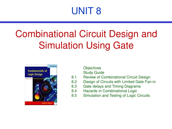
UNIT 8 Combinational Circuit Design and Simulation Using Gate Objectives Study Guide Review of Combinational Circuit Design Design of Circuits with Limited Gate Fan-in Gate delays and Timing Diagrams Hazards in Combinational Logic Simulation and Testing of Logic Circuits 8.1 8.2 8.3 8.4 8.5
Objectives Topics introduced in this chapter: Draw a timing diagram for a combinational circuit with gate delays. Define static 0-and 1-hazards and dynamic hazard. Given a combinational circuit, find all of the static 0-and 1-hazards. For each hazard,specify the order in which the gate outputs must switch in order for the hazard to actually produce a false output. Given switching function, realize it using a two-level circuit which is free of static and dynamic hazards (for single input variable changes). Design a multiple-output NAND or NOR circuit using gates with limited fan-in. Explain the operation of a logic simulator that uses four-valued logic. Test and debug a logic circuit design using a simulator.
8.2 Design of Circuits with Limited Gate Fan-in Example: Realize the functions given in Figure 8-2, using only 2-input NAND gates and inverters. If we minimize each function separately,the result is = = = + + + + ' ' ' ' ' ' f f f b c ab a b b c bc a b a b c ab bc + ' ' 1 ' 2 + ' 3 Figure 8 Figure 8- -2 2
8.4 Hazards in Combinational Logic Detection of a 1-Hazard Assume: Each gate has 10 ns pro. delay time A = C = 1 Hazard occurs when B changes while A = C = 1
8.4 Hazards in Combinational Logic Detection of a Static 0-Hazard = A C A D + )( ' ' A F = + ' + B C D + ')( ' AD + + ( ' ) F ' ' C BCD Four pairs of adjacent 0 s that are not covered by a common loop
8.4 Hazards in Combinational Logic Detection of a Static 0-Hazard What happens if C changes from 0 to I when A=0, B=1, D=0 Assume that propagation delay time is each inverter: 3 ns, AND/OR gate: 5 ns
8.4 Hazards in Combinational Logic Detection of a Static 0-Hazard C changes from 0 to 1 when A=0, B=1, D=0 Inverter: 3 ns, AND/OR gate: 5 ns
8.4 Hazards in Combinational Logic Karnaugh Map Removing Hazards = A C A D + )( ' + B C D C + + ')( ' + + B D A B C + ' )( ' + + ( ' )( ')( ' ') F D A
8.5 Simulation and Testing of Logic Circuit AND and OR Functions for Four-Valued Simulation 0 1 X Z 0 1 X Z 0 X X X + 0 1 X Z 0 1 X Z X 1 X X 0 0 0 0 0 1 X X 0 X X X 0 1 1 1 1 1 1 1 X 1 X X