Complete Review of MOS Transistor Operation and Models in Analog Circuit Design
Explore the operation regions of MOS transistors, including saturation, ohmic, and subthreshold regions. Learn about the small-signal and large-signal behavior, as well as frequency-dependent models in analog circuit design. Dive into practical examples and understand various amplifier configurations for effective circuit design.

Download Presentation

Please find below an Image/Link to download the presentation.
The content on the website is provided AS IS for your information and personal use only. It may not be sold, licensed, or shared on other websites without obtaining consent from the author. If you encounter any issues during the download, it is possible that the publisher has removed the file from their server.
You are allowed to download the files provided on this website for personal or commercial use, subject to the condition that they are used lawfully. All files are the property of their respective owners.
The content on the website is provided AS IS for your information and personal use only. It may not be sold, licensed, or shared on other websites without obtaining consent from the author.
E N D
Presentation Transcript
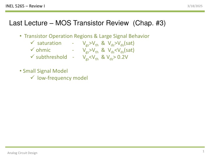
INEL 5265 Review I 3/18/2025 Last Lecture MOS Transistor Review (Chap. #3) Transistor Operation Regions & Large Signal Behavior saturation - Vgs>Vth & Vds>Vds(sat) ohmic - Vgs>Vth & Vds<Vds(sat) subthreshold - Vgs<Vth & Vds> 0.2V Small Signal Model low-frequency model 1 Analog Circuit Design
INEL 5265 Review I 3/18/2025 Regions of Operation Saturation Ohmic Subthreshold * For p-channel MOSFET, use n-channel equations with p-channel parameters and invert the current Analog Circuit Design 2
INEL 5265 Review I 3/18/2025 Large Signal MOSFET Model where: VDS(sat) = Vov = o = zero field mobility (cm2/V s) Cox=gate oxide capacitance per unit area (F/cm2) = channel-length modulation parameter (V-1) Vt = Vt0 = zero bias threshold voltage = bulk threshold parameter (1/V0.5) 2| f |= strong inversion surface potential (V) ID0 = process dependant parameter (A) n = subthreshold slope factor Analog Circuit Design 3
INEL 5265 Review I 3/18/2025 MOSFET Small-Signal Model Complete Schematic Model Simplified Schematic Model Analog Circuit Design 4
INEL 5265 Review I 3/18/2025 Small-Signal Frequency Dependent Model Complete Model * The capacitor size varies with the region of operation and the transistor size * The parasitic capacitors are constant for a specific region of operation Analog Circuit Design 5
INEL 5265 Review I 3/18/2025 Frequency Response 6 Analog Circuit Design
INEL 5265 Review I 3/18/2025 Single Stage Amplifiers 7 Analog Circuit Design
INEL 5265 Review I 3/18/2025 Common Source Amplifier = A g R 0r v m D 8 Analog Circuit Design
INEL 5265 Review I 3/18/2025 Common Source Amplifier with Degeneration = A G R r 0 v m g D m = G m + 1 g R m s 9 Analog Circuit Design
INEL 5265 Review I 3/18/2025 Common Gate Amplifier v= A g R 0r m D 10 Analog Circuit Design
INEL 5265 Review I 3/18/2025 Common Drain Amplifier or Voltage Follower 1 = A g Ro v m g m 11 Analog Circuit Design


