Comprehensive Exam 2 Information for Electronics Engineering Students
Prepare for Exam 2 in electronics engineering with this detailed information. Topics include Thevenin and Norton equivalent circuits, high-speed design techniques, transient response, crosstalk, noise margin, packaging options, thermal effects, transmission line parameters, termination schemes, decoupling capacitors, clock sources, oscilloscope characteristics, and more.

Download Presentation

Please find below an Image/Link to download the presentation.
The content on the website is provided AS IS for your information and personal use only. It may not be sold, licensed, or shared on other websites without obtaining consent from the author. If you encounter any issues during the download, it is possible that the publisher has removed the file from their server.
You are allowed to download the files provided on this website for personal or commercial use, subject to the condition that they are used lawfully. All files are the property of their respective owners.
The content on the website is provided AS IS for your information and personal use only. It may not be sold, licensed, or shared on other websites without obtaining consent from the author.
E N D
Presentation Transcript
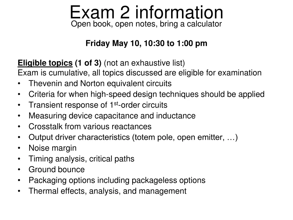
Exam 2 information Open book, open notes, bring a calculator Friday May 10, 10:30 to 1:00 pm Eligible topics (1 of 3) (not an exhaustive list) Exam is cumulative, all topics discussed are eligible for examination Thevenin and Norton equivalent circuits Criteria for when high-speed design techniques should be applied Transient response of 1st-order circuits Measuring device capacitance and inductance Crosstalk from various reactances Output driver characteristics (totem pole, open emitter, ) Noise margin Timing analysis, critical paths Ground bounce Packaging options including packageless options Thermal effects, analysis, and management
Exam 2 information Open book, open notes, bring a calculator Eligible topics (2 of 3)(continued) Transmission line model, parameters of interest, loss mechanisms Transmission line propagation, voltages and currents, reflections Return-path current and crosstalk Ground plane interruptions and routing issues Near-end and far-end crosstalk Power planes and board layer stack up Termination schemes (far end, source end) Real resistor characteristics Via types and specifications Electrical effects of vias Proper via placement for managing return-path current Proper decoupling capacitor placement and connections
Exam 2 information Open book, open notes, bring a calculator Eligible topics (3 of 3)(continued) Bypass capacitor role and placement Real capacitor characteristics Connectors and pin inductance Cables and return current path management EMI and radiated emissions Radiation from common-mode and differential mode currents Pipelining and latency Demultiplexing and multiplexing Clock sources Clock skew and fine timing adjustments Oscilloscope characteristics Passive and active probes Test procedures and design for test
Exam 2 information Open book, open notes, bring a calculator Specific topics (not an exhaustive list) Board layer stack, return-path current management, and decoupling capacitors Daisy chain signal routing and end termination placement Signal routing and termination placement EMI characteristics of common-mode and differential-mode currents High frequency behavior of real components Near-end and far-end crosstalk issues How risetime impacts HSD performance 7 problem sets, total of 16 questions 3 ask for solutions, 7 are multiple choice, 5 ask for an explanations or descriptions 2 require drawing