Comprehensive Guide to Semiconductors: Types, Doping, and Conductivity
"Explore the world of semiconductors with this comprehensive guide covering intrinsic and extrinsic materials, N-type and P-type semiconductors, doping processes, and current flow mechanisms. Learn about the properties and classifications of semiconductors in this insightful seminar submission."

Download Presentation

Please find below an Image/Link to download the presentation.
The content on the website is provided AS IS for your information and personal use only. It may not be sold, licensed, or shared on other websites without obtaining consent from the author. If you encounter any issues during the download, it is possible that the publisher has removed the file from their server.
You are allowed to download the files provided on this website for personal or commercial use, subject to the condition that they are used lawfully. All files are the property of their respective owners.
The content on the website is provided AS IS for your information and personal use only. It may not be sold, licensed, or shared on other websites without obtaining consent from the author.
E N D
Presentation Transcript
www.studymafia.org Seminar On Semiconductors Submitted To: www.studymafia.org www.studymafia.org Submitted By:
Content Introduction Types OF Semiconductors Intrinsic Extrinsic N-Type Material P-Type material Classification of materials Band diagram Current flow in semiconductor References
Introduction Semiconductors are materials which have a conductivity between conductors (generally metals) and nonconductors or insulators (such as most ceramics). Semiconductors can be pure elements, such as silicon or germanium, or compounds such as gallium arsenide or cadmium selenide. In a process called doping, small amounts of impurities are added to pure semiconductors causing large changes in the conductivity of the material.
TYPES OF SEMICONDUCTORS Extrinsic P- type material Semiconduktor Intrinsic N-type material
Intrinsic An intrinsic (pure) semiconductor, also called an undoped semiconductor or i-type semiconductor, is a pure semiconductor without any significant dopant species present. The number of charge carriers is therefore determined by the properties of the material itself instead of the amount of impurities.
EXTRINSIC Created when an impure atom is diffused or implanted into an intrinsic semiconductor. The process of diffusion or implantation impurities an the atom is known as doping. The purpose of doping is to increase the number of electron/holes to improve the conductivity of extrinsic
N-Type Material An n-type semiconductor is an intrinsic semiconductor doped with phosphorus (P), arsenic (As), or antimony (Sb) as an impurity. Silicon of Group IV has four valence electrons and phosphorus of Group V has five valence electrons. If a small amount of phosphorus is added to a pure silicon crystal, one of the valence electrons of phosphorus becomes free to move around (free electron*) as a surplus electron. When this free electron is attracted to the + electrode and moves, current flows.
P-Type material In a pure (intrinsic) Si or Ge semiconductor, each nucleus uses its four valence electrons to form four covalent bonds with its neighbors (see figure below). Each ionic core, consisting of the nucleus and non-valent electrons, has a net charge of +4, and is surrounded by 4 valence electrons. Since there are no excess electrons or holes In this case, the number of electrons and holes present at any given time will always be equal.
Classification of materials Atomic structure consists of three basic element: o Proton o Neutron o Electron Proton and neutron make up the nucleus. Electron spin in the orbit around the nucleus. Electrons are negatively charged and protons are positively charged. Atom is neutral when the value of proton and electron is equal. Neutron and proton has the same mass. The number of neutron in a nucleus determines the weight of an atom.
BOHRS THEORY According to Bohr's theory, electron orbit around the nucleus at a specific energy level. The orbit or shell that used by the electrons to orbit around the nucleus is labelled K,L,M and N. The number of electron in each orbit is given by the formula 2n , with n representing the orbit number of shell position from the nucleus (that is n=1, 2, 3, ) Shell 1 = K Shell 2 = L Shell 3 =M Valence electron have the highest energy level. The number of valence electron is the different between the total electron in an atom and the total electron in orbit K, L, and M. The number of valence electron determines the classification of the element. The classification are classified into three type based on its ability to conduct current. ( conductor, insulator and semiconductor)
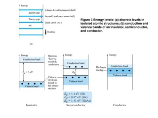
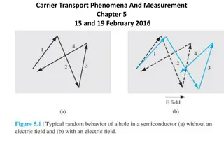
Band diagram Electron in orbit contain kinetic and electric potential energy. Orbit of atom are referred to as energy levels. Random movement of electron in orbit is influenced by the combination of the electric field of atom and other nearby atoms.
We will resolve the discussion of solids into three types, where bands are concerned:
Insulator An insulator is a material that does not conduct electrical current. Insulating materials include paper, plastic, rubber, glass and air. Vacuum is also an insulator, but is not actually a material. Most electrical conductors are covered by insulation. Magnet wire is coated with an extremely thin layer of insulation so that more turns or larger wire may be used in the winding of transformers etc.
Semiconductor semiconductors there is a small enough gap between the valence and conduction bands that thermal or other excitations can bridge the gap. With such a small gap, the presence of a small percentage of a doping material can increase conductivity dramatically. where there is no conductivity at absolute zero and conductivity increases as temperature increases
Conductor conductors like metals the valence band overlaps the conduction band, where the electrons in the highest energy levels are free to move along delocalized energy levels. Conductivity decreases as the temperature is raised.
Current flow in semiconductor N-type Materials P-type Materials Occur simultaneously in two ways: i. Flow of holes in the valence band which is the majority current carrier, ii.Flow of free electron in the conduction band which is the minority current carrier. Occur simultaneously in two ways: i. Flow of free electron in the conduction band which is the majority current carrier ii.Flow of holes in valence band which is the minority current carrier
CURRENT FLOW IN N-TYPE MATERIALS
N-Types extrinsic semiconductor connected to a voltage source. Electrons move to positive terminal of the voltage source. Holes left behind because of the movement of the electron in the valence band seem to move to the negative terminal of the voltage source. In N-types material, most of current is due to electron because they are majority carrier. While holes are the minority carrier in N-types materials, thus the current due to holes is minimal. When the temperature of the semiconductor is increased, more holes will be formed due to thermal energy. The minority current from holes will increase.
Holes repelled by the positive terminal of the voltage source will move towards the negative terminal of the voltage source. Free electron will move to the positive terminal of the voltage source. Current in N-type materials is greater than the current in the P-type materials because the electron movement in the conduction band is much easier compared to holes movement in the valence band.
Pn junction i. .
i. When the two materials P-types and N-Types are combined they formed a PN junction. ii. The different structure of P-types and N-types materials allows the creation of devices such as diodes, unijunction transistor, bipolar junction transistor and field effect transistor
References www.google.com www.wikipedia.com www.studymafia.org