Current Mirrors in Analog Circuit Design: Key Concepts and Practical Considerations
Explore the intricacies of current mirrors in analog circuit design, covering topics such as threshold voltage mismatch, conductance parameter mismatch, and practical design problems. Learn techniques to optimize performance and reduce mismatch effects for enhanced circuit functionality.

Download Presentation

Please find below an Image/Link to download the presentation.
The content on the website is provided AS IS for your information and personal use only. It may not be sold, licensed, or shared on other websites without obtaining consent from the author. If you encounter any issues during the download, it is possible that the publisher has removed the file from their server.
You are allowed to download the files provided on this website for personal or commercial use, subject to the condition that they are used lawfully. All files are the property of their respective owners.
The content on the website is provided AS IS for your information and personal use only. It may not be sold, licensed, or shared on other websites without obtaining consent from the author.
E N D
Presentation Transcript
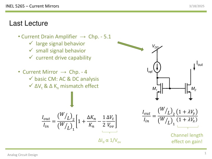
INEL 5265 Current Mirrors 3/18/2025 Last Lecture Current Drain Amplifier Chp. - 5.1 large signal behavior small signal behavior current drive capability VDD Iout Iref Current Mirror Chp. - 4 basic CM: AC & DC analysis Vt& Kn mismatch effect M1 M2 ?? 2 ??1 1 + ??? 1 + ??? ???? ??? ?? 2 ??1 = ???? ??? 1 + ?? 1 ?? ??? = ?? 2 Channel length effect on gain! Id 1/Vov 1 Analog Circuit Design
INEL 5265 Current Mirrors 3/18/2025 Vt Mismatch Experimental Data Threshold voltage variability exhibits a Gaussian behavior! ??? ?? ? ??= To reduce the Vt mismatch by 1/2 takes 4 times the area! Reference: Marcel J. M. Pelgrom, Matching properties of MOS transistors, IEEE JSSC, Oct. 1989 2 Analog Circuit Design
INEL 5265 Current Mirrors 3/18/2025 Conductance Parameter Mismatch ? ? ? ?? ?? = To reduce the k mismatch by 1/2 takes 4 times the area! Reference: Marcel J. M. Pelgrom, Matching properties of MOS transistors, IEEE JSSC, Oct. 1989 3 Analog Circuit Design
INEL 5265 Current Mirrors 3/18/2025 Problem #1 For the following current mirror: a) Find the maximum value of Iref such that M2 still works in saturation. b) Assuming Iref has a voltage drop of 0.2V, find the minimum value possible for Vdd. VDD where Iout VT0n=|VT0p|=0.7V K n=100 A/V2 K p=25 A/V2 n= p =0 Iref Vy M1 M2 VDD=3.3V Iout=4Iref (W/L)2=8 Vy = [0.4 - 3.0]V 4 Analog Circuit Design
INEL 5265 Current Mirrors 3/18/2025 VDD Iout If VDSmin=0.4V=VDSSAT Iout=100uA/V2 8(0.4)2 Iout=64uA Iref=16uA + 0.2V - Iref Vy M1 M2 VGS=1.1V For 16uA 5 Analog Circuit Design
INEL 5265 Current Mirrors 3/18/2025 Cascode Current Mirror Iout Cascode Transistor! VDD M4 Vb Iref Vin = Rin = Vout(min) = Rout = M1 M2 M2 =N M1 6 Analog Circuit Design
INEL 5265 Current Mirrors 3/18/2025 Cascode Current Mirror VDD Generates Vb! Iout Iref M3 M4 Vin = Rin = Vout(min) = Rout = M1 M2 M2 =N M1 7 Analog Circuit Design
INEL 5265 Current Mirrors 3/18/2025 Low-Voltage Cascode Current Mirror VDD Iout Iref Vb M4 M3 Vin = Rin = Vout(min) = Rout = M1 M2 M2 =N M1 8 Analog Circuit Design
INEL 5265 Current Mirrors 3/18/2025 Self-Biased Cascode Current Mirror VDD Generates Vb! Iref Iout Rb M3 M4 Vin = Rin = Vout(min) = Rout = M1 M2 M2 =N M1 9 Analog Circuit Design


