Cutting-edge ASPiDeS Project: Advancing High Energy Physics with Digital SiPM Technology
Dive into the innovative ASPiDeS project led by Università di Pavia and INFN Pavia, focusing on developing digital SiPMs in CMOS technology for high-energy physics applications like dual readout calorimetry, RICH, dark matter, and neutrino experiments. Discover the project's goals, participating units, people involved, research areas, and the use of high dynamic range dSiPMs with millimeter-scale silicon photomultipliers. Explore the integration of sensing elements and processing electronics in the common substrate of a CMOS process, and the investigation of dSiPM operation in cryogenic conditions for improved performance in light detectors. Uncover the project's advancements in timing resolution, noise rejection, threshold adjustment, and more, all set to revolutionize the field of high-energy physics.
Download Presentation

Please find below an Image/Link to download the presentation.
The content on the website is provided AS IS for your information and personal use only. It may not be sold, licensed, or shared on other websites without obtaining consent from the author. If you encounter any issues during the download, it is possible that the publisher has removed the file from their server.
You are allowed to download the files provided on this website for personal or commercial use, subject to the condition that they are used lawfully. All files are the property of their respective owners.
The content on the website is provided AS IS for your information and personal use only. It may not be sold, licensed, or shared on other websites without obtaining consent from the author.
E N D
Presentation Transcript
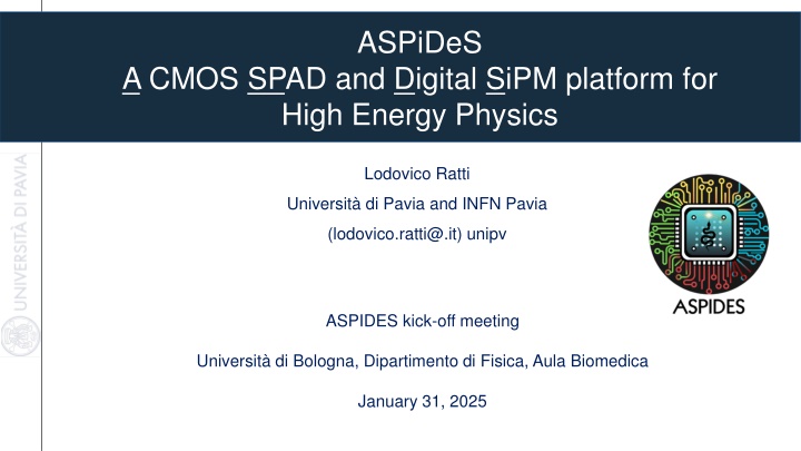
ASPiDeS A CMOS SPAD and Digital SiPM platform for High Energy Physics Lodovico Ratti Universit di Pavia and INFN Pavia (lodovico.ratti@.it) unipv ASPIDES kick-off meeting Universit di Bologna, Dipartimento di Fisica, Aula Biomedica January 31, 2025
ASPIDES project in a nutshell o Goal: develop SiPMs in CMOS technology (digital SiPMs or dSiPMs) for fast (high time density), high dynamic range counting and high accuracy timing application to dual readout calorimetry, RICH, dark matter and neutrino experiments o Participating units: Bari (N. Mazziotta), Bologna (L. Rignanese), Milano (R. Santoro), Pavia (L. Ratti), Trento (L. Pancheri), Napoli (M. Campajola), Padova (G. Collazuol), Torino (M. Da Rocha Rolo) o People involved: 7.85 FTE (27 researchers, 9 technologists) o Research area: Detectors and electronics o Duration: 3 years 2 ASPIDES kick-off meeting, January 31, 2025
High dynamic range dSiPMs o Millimeter scale, 2D monolithic silicon photomultipliers providing o fully digital output obtained through a completely digital processing chain (or, as a possible alternative, through current or charge integration and A/D conversion) o time of arrival of the first bunch of photons and bunch duration with better than 100 ps resolution o threshold adjustment capabilities for noise rejection o possibility of individual micro-cell enabling o asynchronous counting over a more than three decade wide dynamic range of simultaneously firing micro-cells (order of a few thousands, 15/20 micron pitch) o Integration of the sensing element and the processing electronics in the common substrate of a CMOS process is instrumental in accomplishing all of the above features 3 ASPIDES kick-off meeting, January 31, 2025
Light detectors for RICH, dark matter, neutrino physics o Different specifications as compared to DR calorimetry o large SiPM area, few to 10 mm side, but milder granularity requirements better trade- off possible between functional density and PDE o very small signal, setting some demanding specifications on dark count rate operation at low temperature for noise performance improvement o One of the ASPiDeS goals is the investigation of dSiPM operation in cryogenic conditions o modeling of sensor behavior at LN temperature o modeling of transistors and processing circuit behavior at cryogenic temperature o Improvement with decreasing temperature may be limited by BTB or TA tunneling o TCAD simulations to optimize the sensor by reducing weakly temperature dependent contributions to DCR (NDA signed by Napoli, Trento and Pavia to access technology data) 4 ASPIDES kick-off meeting, January 31, 2025
Specifications Requirements SiPM Unit area (mm^2) Dual readout calorimetry Cherenkov (eg RICH, IACT) mm scale DM 10x10 25-30 (maybe larger, to be checked) neutrino 6x6 1x1 Micro-cell pitch (um) 10-15 40-50 50-150 Macro-pixel area (um^2) PDE (%) 500x500 >20 > 40 >45 >35 DCR (kHz) AP (%) <100 kHz/mm2 <1 very low for single pe detection few <0.1 Hz/mm2(at LN) <0.2 Hz/mm2(at LN) <5% Total Correlated Noise Probability (Xtalk + AP) < 60 % self Xtalk (%) Trigger few few self, external <35% external, self no. of fired cells in 1 or 2 time windows (10's of ns long) Output data: light intensity time of arrival of the first photon in the window, possibly of the last photon (TOT) <100 Output data: time Time resolution (ps) ToA and ToT < 100 single pe ToA and TOT strip with 8 units (1mm x 16 mm), pitch of 2 mm BGA Module size and form factor Connection 5 ASPIDES kick-off meeting, January 31, 2025
Possible floorplans for the test chip o 24x4=96 pads (cpga 100) o 24x4=96 pads (cpga 100) o 36x4=144 pads (CPGA 144 package) o very likely pad limited o 20x2+24x2=8 8 pads (cpga 100) o 28x2+24x2=104 pads (cpga 120) 6 ASPIDES kick-off meeting, January 31, 2025
Activity program o Characterization of the ASAP110LF test chip developed in a 110 nm CMOS technology, including different SPAD arrays with different features (passive and active quenching, different active area, structures for investigating timing properties and ionizing radiation tolerance) and mini-SiPMs o DCR, breakdown voltage, afterpulsing, electrical and optical cross-talk, also as a function of the temperature o QE and PDP/PDE o Time resolution 2025 o Investigation of the cumulative damage from ionizing radiation (X- and -ray) and from atomic dislocation in the substrate (neutrons, protons) o Study of SPAD operation in cryogenic conditions 7 ASPIDES kick-off meeting, January 31, 2025
Activity program Development of small scale prototypes of CMOS SiPMs consisting of about 1000 SPADs with o 15-20 um pitch o on sensor electronics to be provided with event detection, counting, thresholding and time stamping capabilities, possibly together with the ability to follow the time evolution of the light pulses reconstruction of the longitudinal shower and discrimination between Cherenkov and scintillation signals specific structures included to test the chip functionalities 2025-26 o submission 3Q/4Q 2025, characterization 1Q 2026 Development of a demonstrator chip including 8 SiPMs, each with a 1 mm2area and a 2 mm o pitch (64x64 cells, 15 um pitch) dual readout calorimetry o inter-SiPM region used for integrating most of the electronics, to minimize the impact on the fill-factor o smaller versions of dSiPMs for application to RICH, DM and neutrino experiments (larger SiPMs) o characterization to be performed in the lab and in a beam test 2026-27 submission 4Q 2026, characterization 2Q-4Q 2027 8 ASPIDES kick-off meeting, January 31, 2025
Device characterization and modeling Some aspects only quickly mentioned in the proposal, but scientifically intriguing and potentially innovative o Radiation damage studies o Not only for technology qualification but also to investigate the underlying damage mechanisms o Both ionization (X and -rays, not so much about this in the literature) and bulk damage o Short- and mid-term annealing during irradiation (neutron and protons) using DCR as a damage probe o Effects on after-pulsing, possible appearance of radiation induced RTS fluctuations o Operation at cryogenic temperatures o Also effects on transistors and electronics o TCAD simulation and modeling o Very low noise operation at cryogenic temperatures o Possibly improved radiation tolerance 9 ASPIDES kick-off meeting, January 31, 2025
Work-package structure o WP1 ASIC design and verification (F. Licciulli, BA) o simulation, layout and verification of the prototype and demonstrator chips o WP2 Testing, data acquisition and integration (R. Santoro, MI) o development of the measurement setup for test, prototype and demonstrator chips o characterization of test, prototype and demonstrator chips o integration of the module and test on a beam line o WP3 Radiation tolerance and cryogenic operation (G. Fiorillo, NA) o radiation tolerance and characterization at cryogenic temperature of the test chip o characterization at cryogenic temperature of the prototype and demonstrator chips o WP4 Sensor characterization, simulation and modeling (L. Pancheri, TN) o simulation and modeling of radiation damage and cryogenic operation, sensor design optimization for low noise operation at cryogenic temperature and improved radiation tolerance o characterization, also after irradiation and at cryogenic temperature, of single micro- cells 10 ASPIDES kick-off meeting, January 31, 2025
Activity plan 11 ASPIDES kick-off meeting, January 31, 2025
Milestones 12 ASPIDES kick-off meeting, January 31, 2025
First year budget o Offers from vendors needed to unlock sj funds (next CSN5 scheduled for May 19-21) o Additional funds cane be requested for oral presentations at conferences 13 ASPIDES kick-off meeting, January 31, 2025
Periodic meetings and more o Weekly online collaboration meetings (no longer than 1 hour) please reply to the wehen2meet poll o Specific WP meetings (organized by WP leaders) when needed o ASPIDES ALFRESCO repository (many already added as collaborators or contributors) o INFN Indico page ASPIDES is present in the experiment category, WP leaders included as managers can setup the agenda for their meetings o ASPIDES members have already expressed their interest in WP activities o Web site needed for the project 14 ASPIDES kick-off meeting, January 31, 2025

