D/A and A/D Conversion in Computer Systems Lab II Exam Review
"Review for Lab 4 in ECE 354 Computer Systems Lab II covering D/A and A/D conversion, analog communication between PICs, importance of analog circuits, ADC transfer function, and digital-analog conversion process."

Download Presentation

Please find below an Image/Link to download the presentation.
The content on the website is provided AS IS for your information and personal use only. It may not be sold, licensed, or shared on other websites without obtaining consent from the author. If you encounter any issues during the download, it is possible that the publisher has removed the file from their server.
You are allowed to download the files provided on this website for personal or commercial use, subject to the condition that they are used lawfully. All files are the property of their respective owners.
The content on the website is provided AS IS for your information and personal use only. It may not be sold, licensed, or shared on other websites without obtaining consent from the author.
E N D
Presentation Transcript
ECE 354 Computer Systems Lab II Lab 4: D/A and A/D Conversion Exam Review
Status Lab 2 reports graded and returned. All grades will be on WebCT shortly Lab 3 Nice job! See comments on next slide Reports due Monday at 5pm Lab 4 WebCT Quiz April 25-27 Demo May 2-3 Exam : Wed April 27, Marston 132, 2:30-4, closed book Covering Lectures/Labs 1,2,3. Review slides and readings. Practice Exam emailed out today 2
Comments on Lab 3 Use terminology correctly!! virtual memory, memory map, memory control signals, strobe, ack, random, error, short, burned chip, code, rotate FSM design State diagram VHDL style User interface, error checking Memory testing Faults, Why PLD? Why Tri-state buffer? PIC software engineering Debug methodology 3
Lab 4 Overview Analog communication between two PICs Uses A/D and D/A Basic functionality Enter character on terminal 1st PIC converts character to analog voltage Analog value transmitted via wire to 2nd PIC 2nd PIC converts voltage back to digital character 2nd PIC displays character on terminal Configurable: PIC sends or receives, how many characters (voltage levels) are allowed PIC MAX232 Sender PIC MAX232 4kOhm CCP1 AN0 Tx Rx . 0.01uF Receiver low-pass filter 4
Why Analog? Not everything is digital! And even digital signaling has analog aspects (!?) Analog circuits and analysis are still necessary Physical phenomena (ie the real world) are usually analog Many sensors are analog (potentiometer, phototransistor, thermo- sensor, microphone) Many actuators are analog (solenoid, speakers) Some signals need to be processed in analog domain before conversion to digital (amplification, filtering, linearization) Requires conversion between analog and digital domain DAC: digital to analog converter ADC: analog to digital converter PIC has both 5
Digital and Analog Conversion ADC transfer function: 10-bit ADC converter 1024 voltage levels between 0V and VREF 10-bit digital value Usually VDD=VREF How does D/A and A/D conversion work? 6
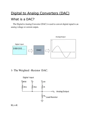
D/A Conversion How can a digital value be converted into a corresponding analog voltage? 7
D/A Conversion Need to generate analog voltage that corresponds to 10-bit digital value PIC uses Pulse Width Modulation (PWM) PWM: Use square wave generator Period and duty cycle adjustable Use low-pass filter to smooth out wave DC value depends on length of duty cycle Shorter period (higher frequency) gives better results PIC Period and duty cycle set through registers 8
Pulse Width Modulation duty cycle VREF pulse width modulated signal 0V period VREF PWM signal, low- pass filtered with short time constant 0V VREF PWM signal, low- pass filtered with long time constant 0V 9
PWM on PIC Registers involved: PR2 register: PWM period CCPR1L and CCP1CON<5:4>: 10-bit duty cycle Basic operation: Start of period Timer TMR2 cleared CCP1 pin set to high 10-bit duty cycle latched to CCPR1H When TMR2 = CCPR1H Clear CCP1 (duty cycle over) When TMR2 = PR2 New period starts 10
Timer 2 Prescaler Prescaler determines effective clock rate for TMR2 Postscaler irrelevant for us Used if Timer 2 needs to drive additional component at different frequency PMW period formula: = ] 1 + OSC [( ) 2 4 ( 2 ) PMW period PR T TMR prescaler 12
PWM Setup Setup steps: Set PWM period by writing to PR2 register Set PWM duty cycle by writing to CCPR1L register and CCP1CON<5:4> bits Make CCP1 pin output by clearing the TRISC<2> bit Set TMR2 prescale value Enable Timer 2 by writing to TCON2 Configure the CCP1 module for PWM operation Example for 20 MHz clock: 13
A/D Conversion How can we generate digital value of analog voltage? 14
A/D Conversion Use D/A converter to generate different analog values and compare Control logic decides which values to try When comparison complete, best match is put on output How can D/A be matched to input in fewest steps? VIN comp D/A converter 10-bit test value start A/D control logic conversion conversion complete clock 10-bit output 15
Successive Approximation Matching strategies: Counting conversion (slow) Successive approximation (faster) Successive Approximation: Basically binary search: 10 steps instead of 1024 XXX XXX <100? 0XX 1XX 0XX <010? 1XX <110? 00X 01X 10X 11X 00X <001? 01X <011? 10X <101? 11X <111? 000 001 010 011 100 101 110 111 16
PIC ADC Characteristics (1) Sample and Hold ADC samples for a given time (charges hold capacitor) Then sample value is disconnected from source ( hold ) A/D conversion is performed On completion, ADC can sample again Sampling takes some time Depends on source impedance (max 10 k ) Lower source impedance reduces sample time because hold capacitance charges faster (see Peatman Figure 10-5(b)) Also depends on temperature, etc. 17
PIC ADC Characteristics (2) Analog input model and acquisition time formula: 18
ADCON0 Register ADC enable (bit 0) Busy/idle (conversion takes some time): Bit 2 in ADCON0 register Check by polling or enable interrupt Channel selection (bits 5-3): Selects pins to be used Selects external or internal reference voltage A/D conversion clock setting (bits 7-6) 19
A/D Conversion Clock Setting Time to convert 1 bit must be 1.6 s Clock setting must be adjusted to external clock 21
ADCON1 Register Port configuration (bits 3-0) Chooses pins to be digital I/O or analog input (see data sheet) Result Format Selection (bit 7) Chooses justification of 10-bit conversion result: 22
ADC Setup 1. Configure A/D module: Configure analog pins/voltage reference and digital I/O (ADCON1) Select A/D input channel (ADCON0) Select A/D conversion clock (ADCON0) Turn on A/D module (ADCON0) 2. Configure A/D interrupt (if desired): Clear ADIF bit Set ADIE bit Set PEIE bit Set GIE bit 3. Wait required acquisition time 4. Start conversion Set GO/_DONE bit (ADCON0) 5. Wait for A/D conversion to complete (polling or interrupt) 6. Read A/D result from (ADRESH:ADRESL) and clear ADIF bit 7. Goto 1. or 2. wait 2 A/D clock ticks 23
Reference PWM (D/A conversion) PIC data sheet pp. 61-62 Peatman Section 6.9 (pp. 112-119) A/D conversion PIC data sheet pp. 111-116 Peatman Chapter 10 24
Lab 4 Lab setup: 2 PICs (available in lab kit) Need 2 terminals PIC PIC MAX232 MAX232 4kOhm CCP1 AN0 Tx Rx . 0.01uF Receiver Sender low-pass filter Send characters coded in analog between terminals Low pass filter needs to be adapted to PWM settings 25
Signal Discretization We use adaptable signal coding Choose between 2x (x={1,2,..6}) symbols: VREF B 21=2 symbols VREF VREF D C ... 22=4 symbols 26=64 symbols B ... A B A A 0V 0V 0V Robustness depends on x: Most robust: only two characters and two voltages 512 ADC results can represent one character Most information: 64 characters and voltage ranges 16 ADC results can represent one character 26
Lab 4 Demo Each PIC can be used for transmitting or receiving User can specify function after reset User also specifies coding level (1..6) Same on both PICs Requires well-designed ASCII manipulation When character is entered on terminal PIC 1 receives character Converts it to analog signal PIC 2 received analog signal Converts it to digital value Prints result on terminal Should be robust for low coding levels 27
Exam Review See last year s exam solutions emailed out today Topics: PIC Architecture Interrupts Serial communication Timers Assembly 28


")
")