Data Analysis on Valid Patterns in TM Structures
In this dataset, images depicting various valid patterns in TM structures are analyzed. The patterns are categorized based on different parameters such as energy offsets and event types. Each image represents a unique set of characteristics for the TM structures, providing valuable insights for further research and analysis in the field of material science. The images showcase different trends and variations in the patterns observed across different time frames, revealing significant information about the properties of the structures.

Download Presentation

Please find below an Image/Link to download the presentation.
The content on the website is provided AS IS for your information and personal use only. It may not be sold, licensed, or shared on other websites without obtaining consent from the author.If you encounter any issues during the download, it is possible that the publisher has removed the file from their server.
You are allowed to download the files provided on this website for personal or commercial use, subject to the condition that they are used lawfully. All files are the property of their respective owners.
The content on the website is provided AS IS for your information and personal use only. It may not be sold, licensed, or shared on other websites without obtaining consent from the author.
E N D
Presentation Transcript
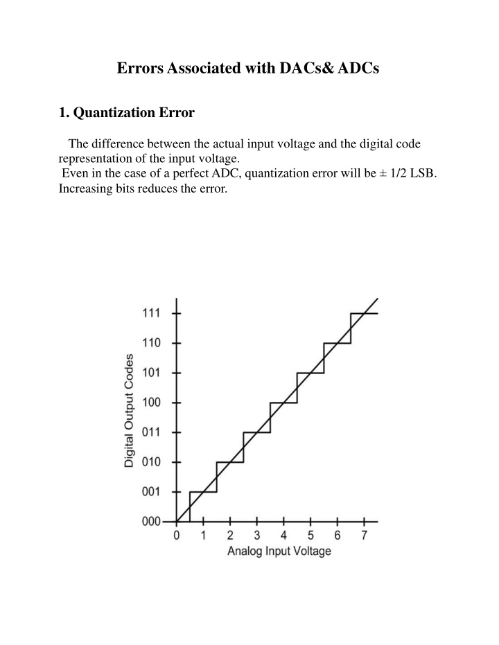
Errors Associated with DACs&ADCs 1. Quantization Error The difference between the actual input voltage and the digital code representation of the input voltage. Even in the case of a perfect ADC, quantization error will be 1/2 LSB. Increasing bits reduces the error.
120 2. Offset Error Offset Error is the difference between the first transition point and the ideal first transition point. (Measured in LSBs). Digital Code Out = A + Vin where Ais the analogue offset error Offset Errors can be corrected in Firmware Correction for offset error and can be made by adding (or subtracting) the correction from each code.
121 3. GainError Full scale range is the difference between the first and last code transition points. The ideal full scale range minus the actual full scale range equals Gain Error. (Measured in LSBs) Digital Code = B VIN where B is the gain error
Gain Errors can be corrected in firmware Corrections for gain error and can be made by multiplying each code by the ratio of ideal to actual full scale range. 122 4. Differential Nonlinearity (DNL) Error DNLis a measure of variations in code widths from the ideal code width.
DNL of LSB implies that: LSB < all code widths < 1 LSB A missing code means DNL = -1LSB 123
5- Missing Codes If the DNL spec goes beyond -1LSB, then missing codes will appear. The term No Missing Codes means that no digital output codes are skipped as the analog input is swept from zero to full scale. Most ADCs today will include the specification No missing codes .