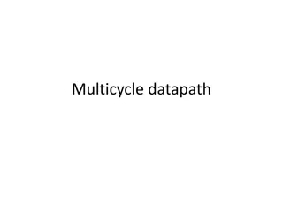
Datapath and Control Timing Insights

In this lecture on Datapath and Control, Prof. Jeffrey Falkinburg discusses the methodology behind designing datapaths and controls in embedded systems. Explore the timing behavior and critical paths in circuits to predict clocking frequencies and understand complex circuit operations. Learn about propagation delays of flip-flops, control word application, and memory input stabilization times.

Download Presentation

Please find below an Image/Link to download the presentation.
The content on the website is provided AS IS for your information and personal use only. It may not be sold, licensed, or shared on other websites without obtaining consent from the author.If you encounter any issues during the download, it is possible that the publisher has removed the file from their server.
You are allowed to download the files provided on this website for personal or commercial use, subject to the condition that they are used lawfully. All files are the property of their respective owners.
The content on the website is provided AS IS for your information and personal use only. It may not be sold, licensed, or shared on other websites without obtaining consent from the author.
E N D
Presentation Transcript
CSCE 436 Advanced Embedded Systems Lecture 12 Datapath and Control Prof Jeffrey Falkinburg Avery Hall 368 472-5120
Lesson Outline Time Logs! HW #7 Due Now! Datapath and Control Timing VHDL Instantiation Keyboard serial to parallel converter 2 CSCE 436 Advanced Embedded Systems
Datapath and Control - Timing 3 CSCE 436 Advanced Embedded Systems
Datapath and Control - Timing Datapath and Control Design Methodology Datapath - responsible for data manipulations Control - responsible for sequencing the actions of the datapath Fig 11.0 - An abstract digital system constructed from a datapath and a control unit. 4 CSCE 436 Advanced Embedded Systems
Datapath and Control - Timing Reasons to examine the timing behavior of a datapath and control circuit. First, so that we can make informed predictions about the expected clocking frequency of our circuits. Second, so that we can identify critical paths in our circuit. Third, so that we can develop our intuition about the operation of these complex circuits. 1. 2. 3. 5 CSCE 436 Advanced Embedded Systems
Datapath and Control - Timing Circuit from Lesson 11 Search algorithm for minimum 6 CSCE 436 Advanced Embedded Systems
Datapath and Control - Timing Tp(A) Tpd(FF) Propagation Delay of Flip Flops FF is input to OEs Tp(B) Qvalid OEs assert their new values Tp(C) SWvalid time difference between the application of a valid control word to the datapath and the status input to the control unit becoming valid 7 CSCE 436 Advanced Embedded Systems
Datapath and Control - Timing Tp(D) Dvalid delay between the status inputs becoming valid and the MIEs becoming valid Tp(E) Tsetup Once the memory inputs have stabilized, they must be allowed some setup time 8 CSCE 436 Advanced Embedded Systems
VHDL Instantiation 9 CSCE 436 Advanced Embedded Systems
VHDL Instantiation Binding - technique of assigning signals in the top- level entity (caller) to the signals in the instance uut: lec10 Generic map(5) PORT MAP ( clk => clk, reset => reset, crtl => crtl, D => loadInput, Q => cntOutput); Signals clk, reset, crtl, D and Q were defined inside the lec10 component signals clk, reset, crtl, loadInput, and cntOutput were defined as signals in the higher-level testbench 10 CSCE 436 Advanced Embedded Systems
VHDL Instantiation We could shorten this instantiation by using the default binding calling convention shown in the code below uut: lec10 Generic map(5) PORT MAP (clk, reset, crtl, loadInput, cntOutput); Important Note: When you use the default binding, the order of the signals must match the exact same order that is defined in the entity description. Generates a more compact instantiation statement. 11 CSCE 436 Advanced Embedded Systems
Unused outputs and open keyword However, we could shorten this instantiation by using the default binding calling convention below: entity compare is generic(N: integer := 4); port(x,y : in unsigned(N-1 downto 0); g,l,e: out std_logic); end compare; Important Note: Note that g=1 when x>y, and l=1 when x<Y and e=1 when x=y example: compare port map (A,B,OPEN, OPEN, equal); Synthesis engine can remove the logic associated with any of the OPEN signals and reduce the resources used on the FPGA. 12 CSCE 436 Advanced Embedded Systems
Subvectors and Concatenation There are times when we will need to rebuild a std_logic_vector from pieces of other vectors. Vector is defined as signal(7 downto 0), you can replace the limits with anything in between to get a small subvector For example, you could ask for signal(5 downto 2) for a 4-bit sub-vector of signal. 13 CSCE 436 Advanced Embedded Systems
Subvectors and Concatenation The concatenation operation, &, is a way to "glue" two vectors together. For example, to build a 8-bit vector you could legally write in VHDL signal(3 downto 1) & signal (7 downto 3); These two concepts come together in the shift register used in the lecture 11 code, which contains the following line of VHDL code. shiftReg <= kbData & shiftReg (10 downto 1); 14 CSCE 436 Advanced Embedded Systems
Keyboard Serial to Parallel Converter 15 CSCE 436 Advanced Embedded Systems
Keyboard Serial to Parallel Converter Nomenclature: Data Input: Data Output: Control: Status: Others: Physical Input: Physical Output: Behavior: PS/2 Keyboard none 1-bit data, nominally logic 1 none none 1-bit clk, nominally logic 1 key press and key release events none When a key is pressed, its 8-bit make code is transmitted. When a key is released, an 8- bit break code is transmitted, immediately followed by the key's 8-bit scan code. 16 CSCE 436 Advanced Embedded Systems
Keyboard Serial to Parallel Converter 17 CSCE 436 Advanced Embedded Systems
Keyboard Serial to Parallel Converter Nomenclature: Data Input: Keyboard scan code reader 1-bit kd data, nominally logic 1 1-bit kd clk, nominally logic 1 Data Output: Control: Status: Others: Behavior: 8-bit scan code none 1-bit busy, nominally logic 0 1-bit clk, nominally logic 1 Interprets the PS/2 keyboard clk and data signal from a keypress event and outputs the associated scan code. The busy signal goes high when the first data bit arrives and stays high until the last data bit is received. Busy is low only when there is a valid scan code on the output. 18 CSCE 436 Advanced Embedded Systems
Keyboard Scan Code Reader Algorithm Looking at the timing diagram and the description on previous slide, we get the following algorithm. 1. while(1) { 2. busy=0; 3. while (kb_clk == 1); 4. busy=1; 5. for (count=0 count<33; count++) { 6. while(kb_clk == 1); 7. shift = (shift << 1) | kb_data; 8. while(kb_clk == 0); 9. } // end for 10. scan = shift[9-2] 11. } // end while 1 19 CSCE 436 Advanced Embedded Systems
Homework #8 Now lets build the datapath and control using the technique learned in lecture 11. Your homework is to build the control unit for the keyboard scancode reader. 20 CSCE 436 Advanced Embedded Systems