Design of Mixed Signal Circuits
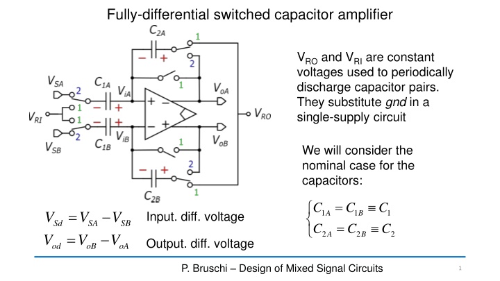
Fully-differential switched capacitor amplifier using constant voltages for discharging capacitor pairs in a single-supply circuit. Analysis of phases, transitions, and voltage outputs are discussed according to the nominal capacitor values.

Download Presentation

Please find below an Image/Link to download the presentation.
The content on the website is provided AS IS for your information and personal use only. It may not be sold, licensed, or shared on other websites without obtaining consent from the author.If you encounter any issues during the download, it is possible that the publisher has removed the file from their server.
You are allowed to download the files provided on this website for personal or commercial use, subject to the condition that they are used lawfully. All files are the property of their respective owners.
The content on the website is provided AS IS for your information and personal use only. It may not be sold, licensed, or shared on other websites without obtaining consent from the author.
E N D
Presentation Transcript
Fully-differential switched capacitor amplifier VROand VRIare constant voltages used to periodically discharge capacitor pairs. They substitute gnd in a single-supply circuit We will consider the nominal case for the capacitors: = = C C C C C C = 1 1 1 V V V A B Input. diff. voltage Sd SA SB = 2 2 2 A B V V V Output. diff. voltage od oB oA P. Bruschi Design of Mixed Signal Circuits 1
Phase 1 v (1) n (1) n v v = + = (1) iA (1) iB ; CMO V v CMO V 2 2 Due to the unity-gain connection Let us write the voltages across each capacitor ) 1 ( n v = + ) 1 ( C v CMO V V 1 A RI 2 ) 1 ( n v = ) 1 ( C v CMO V V 1 B RI 2 ) 1 ( n v = ) 1 ( C v V CMO V 2 A RO 2 ) 1 ( n v = + ) 1 ( C v V CMO V 2 B RO 2 P. Bruschi Design of Mixed Signal Circuits 2
Transition to phase 2 Q Q C Q C Q = + (2) C A v (1) C A v In this analysis we will neglect the kT/C noise, for simplicity 2 A 2A JA 2 2 2 Q 1A = + (2) C B v (1) C B v 2 B 2 2 2 unknown Q 1B (2) n (2) n v v = + = (2) iA (2) ic (2) iB (2) ic ; v V v V Q 2 2 Q 2B QjA, QJB: caused by charge-injection and other mechanisms ) 2 ( v JB = + ) 2 ( 1 ) 2 ( n 2 ) 2 ( v V V ( ( ) ) C A ic SA = (2) 1 C A (1) C A v = = C v Q Q Q Q Q Q Q 1 1 JA 2 1 A A JA v = ) 2 ( 1 ) 2 ( n 2 v V V = (2) 1 C B (1) C B v C v Q C B ic SB 2 1 B B JB 1 1 JB P. Bruschi Design of Mixed Signal Circuits 3
Phase 1 Q C Q C = + (2) C A v (1) C A v Phase 2 2 A ) 1 ( n v 2 2 = + ) 1 ( C v CMO V V 2 1 A RI ) 2 ( v 2 ) 1 ( n v = + ) 2 ( 1 ) 2 ( n 2 ) 2 ( v V V = + (2) C B v (1) C B v 2 B C A ic SA = 2 2 ) 1 ( C v CMO V V 1 B RI 2 v 2 = ) 2 ( 1 ) 2 ( n 2 v V V ( ( ) ) ) 1 ( n v C B ic SB = (2) 1 C A (1) C A v Q C v Q = ) 1 ( C v V CMO V 2 1 1 A JA 2 A RO 2 ) 1 ( n v = (2) 1 C B (1) C B v Q C v Q = + ) 1 ( C v V CMO V 2 1 1 B JB 2 B RO 2 (1) n (2) n (1) n v v v Q C C C = + + + (2) C A v (2) ic JA V CMO V 1 V V CMO V V 2 RO SA RI 2 2 2 2 2 (1) n (2) n (1) n v v v Q C C C = + + + + (2) C B v (2) ic JB V CMO V 1 V V CMO V V 2 RO SB RI 2 2 2 2 2 P. Bruschi Design of Mixed Signal Circuits 4
(1) n (2) n (1) n v v v Q C C C = + + + (2) C A v (2) ic JA V CMO V 1 V V CMO V V 2 RO SA RI 2 2 2 2 2 (1) n (2) n (1) n v v v Q C C C = + + + + (2) C B v (2) ic JB V CMO V 1 V V CMO V V 2 RO SB RI 2 2 2 2 2 = = + + (2) oA (2) iA (2) C A v v v v 2 (2) oB (2) iB (2) C B v v 2 (2) n (2) n v v = + = (2) iA (2) ic (2) iB (2) ic ; v V v V 2 2 P. Bruschi Design of Mixed Signal Circuits 5
(2) n (1) n (2) n (1) n v v v v Q C C C = + + + + + (2) oA (2) ic (2) ic JA v V V CMO V V V CMO V V 1 RO SA RI 2 2 2 2 2 2 + (2) n (1) n (2) n (1) n v v v v Q C C C = + + + + + (2) oB (2) ic (2) ic 1 JB v V V CMO V V V CMO V V RO SB RI 2 2 2 2 2 2 = (2) od (2) oB (2) oA Differential mode analysis v v v Q Q C C ( ) = + + + + (2) od (2) n (1) n (2) n (1) n JB JA v v v 1 v V V v SA SB C 2 2 Q Q C C C C ) ( ) ( = + (2) od (2) n (1) n 1 JB JA v V V v v 1 1 SA SB C 2 2 2 P. Bruschi Design of Mixed Signal Circuits 6
Q Q C C C C ) ( ) ( = + (2) od (2) n (1) n 1 JB JA v V V v v 1 1 SA SB C 2 2 2 V Sd output noise due to the amplifier output error due to charge injection C C = A 1 A dd 2 + Q Q 1 A ( ) (2) n (1) n JB JA v v Errors referred to the input C A 1 Note that CDS is applied to the amplifier noise P. Bruschi Design of Mixed Signal Circuits 7
Common mode components 1 2 1 2 (2) n (1) n (2) n (1) n v v v v Q C C C = + + + + + (2) oA (2) ic (2) ic JA v V V CMO V V V CMO V V 1 RO SA RI 2 2 2 2 2 2 (2) n (1) n (2) n (1) n v v v v Q C C C = + + + + + (2) oB (2) ic (2) ic 1 JB v V V CMO V V V CMO V V RO SB RI 2 2 2 2 2 2 Neglecting the charge injection (calculation of the CM components require less accuracy) + V V C C = + + + (2) ic (2) ic SA SB CMO V V V CMO V 1 V CMO V V RO RI 2 2 C C ( ) ( ) ( ) = + + + + + (2) ic 1 1 CMO V V A V CMO V A 1 V V RO SC RI 2 P. Bruschi Design of Mixed Signal Circuits 8
Common mode components C C ( ) ( ) ( ) = + + + + + (2) ic 1 1 CMO V V A V CMO V A 1 V V RO SC RI 2 C C ( ) ( ) ( ) + + + = + (2) ic 1 1 CMO V V CMO V A 1 V V V A RO SC RI 2 + CMO V V A + ( ) = + + (2) ic RO V CMO V V V SC RI 1 1 A A Since in phase 1 Vicis equal to VCMO, it is desirable that it does not change passing into phase 2. This is not always possible to guarantee, since the common mode of the source may be not predictable = = V V CMO V V To obtain this, we set: RO RI SC P. Bruschi Design of Mixed Signal Circuits 9
Programmable gain amplifier (PGA) C C = A 1 L 2 Capacitors can be made easily programmable. The advantage with respect of resistive feedback amplifier is that the switch resistance does not affect accuracy (it affects only speed) P. Bruschi Design of Mixed Signal Circuits 10
Additional charge injection from non-constant Vic = (1) ic V CMO V = = Q V C + CMO V V A + ( ) = + + (2) ic RO V CMO V V V A ic pA SC RI 1 1 A A Q V C B ic pB In this simplified picture, switches and feedback capacitors are not represented These charges contribute to QJA and QJBtogether with charge injection from the switches Since parasitic capacitance may have some mismatch, a differential voltage may result. P. Bruschi Design of Mixed Signal Circuits 11


")