Devices Specification Table for LM75A, LM75B, LM75C, TMP75, TMP175, TMP275
Explore the detailed specifications, operating voltage ranges, and temperature ranges of LM75A, LM75B, LM75C, TMP75, TMP175, and TMP275 devices. Find information on operating voltage, temperature ranges, quiescent current, bit resolutions, conversion times, and accuracy for various models. Discover pin-out configurations and register maps, as well as power supply ranges and absolute maximum voltages. Dive into the configuration registers for LM75A, LM75B, LM75C, TMP75, TMP175, and TMP275 to understand fault queues, polarity, shutdown options, and more.

Download Presentation

Please find below an Image/Link to download the presentation.
The content on the website is provided AS IS for your information and personal use only. It may not be sold, licensed, or shared on other websites without obtaining consent from the author. If you encounter any issues during the download, it is possible that the publisher has removed the file from their server.
You are allowed to download the files provided on this website for personal or commercial use, subject to the condition that they are used lawfully. All files are the property of their respective owners.
The content on the website is provided AS IS for your information and personal use only. It may not be sold, licensed, or shared on other websites without obtaining consent from the author.
E N D
Presentation Transcript
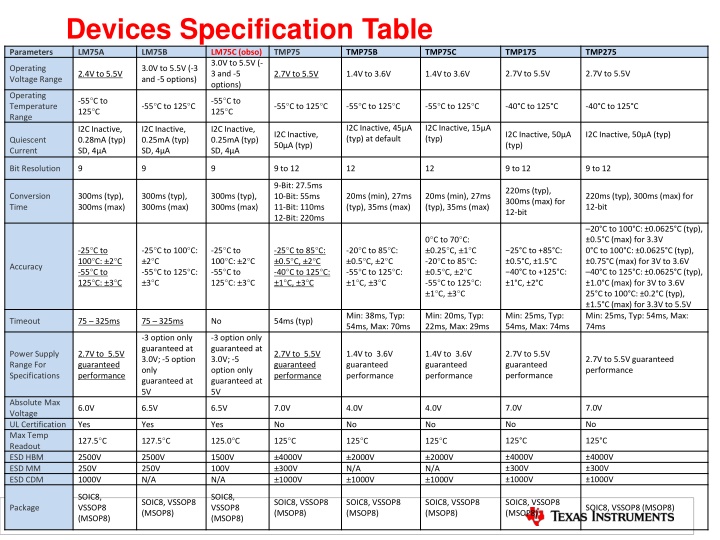
Devices Specification Table LM75A LM75B LM75C (obso) 3.0V to 5.5V (- 3 and -5 options) Parameters TMP75 TMP75B TMP75C TMP175 TMP275 Operating Voltage Range 3.0V to 5.5V (-3 and -5 options) 2.7V to 5.5V 2.7V to 5.5V 2.4V to 5.5V 2.7V to 5.5V 1.4V to 3.6V 1.4V to 3.6V Operating Temperature Range -55 C to 125 C -55 C to 125 C -55 C to 125 C -55 C to 125 C -55 C to 125 C -55 C to 125 C -40 C to 125 C -40 C to 125 C I2C Inactive, 45 A (typ) at default I2C Inactive, 15 A (typ) I2C Inactive, 0.28mA (typ) SD, 4 A I2C Inactive, 0.25mA (typ) SD, 4 A I2C Inactive, 0.25mA (typ) SD, 4 A I2C Inactive, 50 A (typ) I2C Inactive, 50 A (typ) I2C Inactive, 50 A (typ) Quiescent Current 9 to 12 9 to 12 Bit Resolution 9 9 9 9 to 12 12 12 9-Bit: 27.5ms 10-Bit: 55ms 11-Bit: 110ms 12-Bit: 220ms 220ms (typ), 300ms (max) for 12-bit Conversion Time 300ms (typ), 300ms (max) 300ms (typ), 300ms (max) 300ms (typ), 300ms (max) 20ms (min), 27ms (typ), 35ms (max) 20ms (min), 27ms (typ), 35ms (max) 220ms (typ), 300ms (max) for 12-bit 20 C to 100 C: 0.0625 C (typ), 0.5 C (max) for 3.3V 0 C to 100 C: 0.0625 C (typ), 0.75 C (max) for 3V to 3.6V 40 C to 125 C: 0.0625 C (typ), 1.0 C (max) for 3V to 3.6V 25 C to 100 C: 0.2 C (typ), 1.5 C (max) for 3.3V to 5.5V Min: 25ms, Typ: 54ms, Max: 74ms 0 C to 70 C: 0.25 C, 1 C -20 C to 85 C: 0.5 C, 2 C -55 C to 125 C: 1 C, 3 C -25 C to 100 C: 2 C -55 C to 125 C: 3 C -25 C to 100 C: 2 C -55 C to 125 C: 3 C -25 C to 100 C: 2 C -55 C to 125 C: 3 C -25 C to 85 C: 0.5 C, 2 C -40 C to 125 C: 1 C, 3 C -20 C to 85 C: 0.5 C, 2 C -55 C to 125 C: 1 C, 3 C 25 C to +85 C: 0.5 C, 1.5 C 40 C to +125 C: 1 C, 2 C Accuracy Min: 38ms, Typ: 54ms, Max: 70ms Min: 20ms, Typ: 22ms, Max: 29ms Min: 25ms, Typ: 54ms, Max: 74ms Timeout 75 325ms 75 325ms No 54ms (typ) -3 option only guaranteed at 3.0V; -5 option only guaranteed at 5V -3 option only guaranteed at 3.0V; -5 option only guaranteed at 5V Power Supply Range For Specifications 2.7V to 5.5V guaranteed performance 2.7V to 5.5V guaranteed performance 1.4V to 3.6V guaranteed performance 1.4V to 3.6V guaranteed performance 2.7V to 5.5V guaranteed performance 2.7V to 5.5V guaranteed performance Absolute Max Voltage UL Certification Max Temp Readout ESD HBM ESD MM ESD CDM 7.0V 7.0V 6.0V 6.5V 6.5V 7.0V 4.0V 4.0V No No Yes Yes Yes No No No 127.5 C 127.5 C 125.0 C 125 C 125 C 125 C 125 C 125 C 4000V 300V 1000V 2000V N/A 1000V 2000V N/A 1000V 4000V 300V 1000V 4000V 300V 1000V 2500V 250V 1000V 2500V 250V N/A 1500V 100V N/A SOIC8, VSSOP8 (MSOP8) SOIC8, VSSOP8 (MSOP8) SOIC8, VSSOP8 (MSOP8) SOIC8, VSSOP8 (MSOP8) SOIC8, VSSOP8 (MSOP8) SOIC8, VSSOP8 (MSOP8) SOIC8, VSSOP8 (MSOP8) SOIC8, VSSOP8 (MSOP8) Package
Devices Pin Out Pin Out LM75A LM75B LM75C TMP75 TMP75B TMP75C TMP175 TMP275 SDA SDA 1 SDA SDA SDA SDA SDA SDA SCL SCL 2 SCL SCL SCL SCL SCL SCL ALR T GN D A2 A1 A0 Vs ALRT ALRT 3 O.S. O.S. O.S. ALERT ALRT GN D A2 A1 A0 +Vs GN D A2 A1 A0 +Vs GND GND 4 GND GND GND A2 A1 A0 V+ A2 A1 A0 V+ 5 6 7 8 A2 A1 A0 +Vs A2 A1 A0 V+ A2 A1 A0 Vs 2
Register Maps LM75A LM75B LM75C TMP75 TMP75B TMP75C TMP175 TMP275 Registers Name 0x00 0x01 0x00 0x01 0x00 0x01 0x00 0x01 0x00 0x01 0x00 0x01 0x00 0x01 0x00 0x01 Temperature Configuration 0x02 0x02 0x02 X X X X X ????? 0x03 0x03 0x03 X X X X X ??? 0x07 X X X X X Product ID ???? ????? One-shot 0x02 0x03 X 0x02 0x03 X 0x02 0x03 0x04 0x02 0x03 0x02 0x03 3
Configuration Register Configuration Register D7 D6 D5 D4 D3 D2 D1 D0 LM75A 0 0 0 Fault Queue OS Polarity CMP/INT Shutdown LM75B 0 0 0 Fault Queue OS Polarity CMP/INT Shutdown LM75C 0 0 0 Fault Queue OS Polarity CMP/INT Shutdown TMP75 OS R1 R0 F1 F0 POL TM SD TMP175 OS R1 R0 F1 F0 POL TM SD TMP275 OS R1 R0 F1 F0 POL TM SD TMP75B TMP75C OS RSVD CR FQ FQ POL POL TM TM SD SD RSVD OS 4
????? Register ????? Register D15 D14 D13 D12 D11 D10 D9 D8 D7 D6 D5 D4 D3 D2 D1 D0 1 1 1 0 0 0 X X X X X X X X X X X X X X X X X X X X X LM75A LM75B LM75C TMP75 TMP175 TMP275 TMP75B TMP75C 0 0 0 1 1 1 0 0 0 0 0 0 1 1 1 0 0 0 1 1 1 TMPs has ????? and ????, but similar behavior and functionality. 5
??? Register ??? Register D15 D14 D13 D12 D11 D10 D9 D8 D7 D6 D5 D4 D3 D2 D1 D0 0 0 0 0 0 0 X X X X X X X X X X X X X X X X X X X X X LM75A LM75B LM75C TMP75 TMP175 TMP275 TMP75B TMP75C 0 0 0 1 1 1 0 0 0 1 1 1 0 0 0 0 0 0 0 0 0 TMPs has ????? and ????, but similar behavior and functionality. 6