Electromigration Signoff Methodology in Adaptive Voltage Scaling Environment
Explore a comprehensive methodology for electromigration signoff in the presence of adaptive voltage scaling, focusing on bias temperature instability and electromigration effects in interconnects. Learn how adaptive voltage scaling can offset performance degradation and ensure circuit timing requirements are met amidst aging and degradation challenges.
Download Presentation

Please find below an Image/Link to download the presentation.
The content on the website is provided AS IS for your information and personal use only. It may not be sold, licensed, or shared on other websites without obtaining consent from the author. If you encounter any issues during the download, it is possible that the publisher has removed the file from their server.
You are allowed to download the files provided on this website for personal or commercial use, subject to the condition that they are used lawfully. All files are the property of their respective owners.
The content on the website is provided AS IS for your information and personal use only. It may not be sold, licensed, or shared on other websites without obtaining consent from the author.
E N D
Presentation Transcript
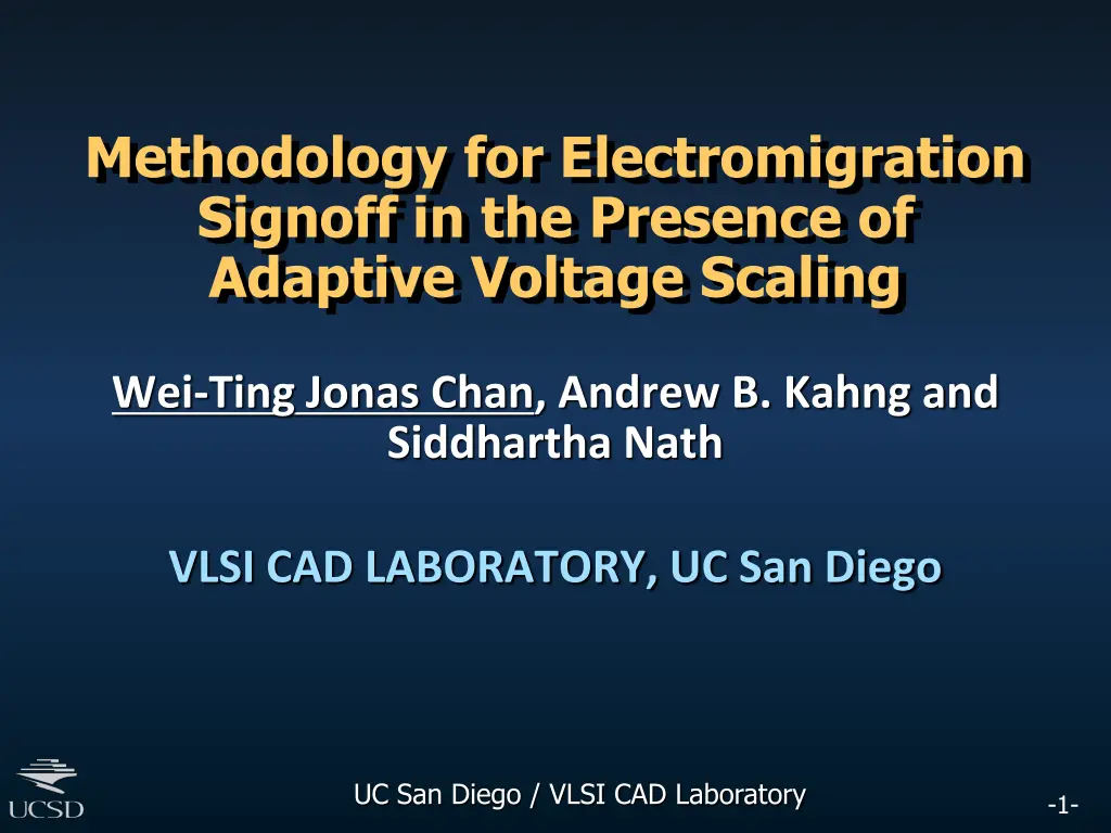
Methodology for Electromigration Signoff in the Presence of Adaptive Voltage Scaling Wei-Ting Jonas Chan, Andrew B. Kahng and Siddhartha Nath VLSI CAD LABORATORY, UC San Diego UC San Diego / VLSI CAD Laboratory -1-
Outline Motivation Previous Work Analysis Models Experimental Setup and Results Conclusions -2-
Bias Temperature Instability (BTI) | Vth| increases when device is on (stressed) | Vth| is partially recovered when device is off (relaxed) |Vgs| ON OFF ON OFF time Device aging (| Vth|) accumulates over time NBTI: PMOS PBTI: NMOS -3- [VattikondaWC06]
Electromigration in Interconnects Electromigration (EM) is the gradual displacement of metal atoms in an interconnect Iavgcauses DC EM and affects power delivery networks Irmscauses AC EM and affects clock and logic signals -4-
Adaptive Voltage Scaling (AVS) Accumulated BTI higher | Vth| slower circuit AVS can compensate for performance degradation Circuit performance Without AVS With AVS Circuit On-chip aging monitor target time Vdd Voltage regulator Circuit performance time Closed-loop AVS -5-
BTI + AVS Signoff Ensure circuit meets timing requirements under BTI aging Use AVS to offset BTI degradation Step 1 Step 2 Step 3 VBTI | Vt| Circuit Derated library implementation and signoff Vlib ? BTI degradation and AVS Vfinal netlist Signoff loop of BTI -6-
EM + BTI + AVS Signoff? Aggressive AVS scheduling results in more severe degradation Guardband during implementation increases due to degradation EM loop Stress on Wires Design Vfinal Implementation BTI loop Derated Libraries Vlib, VBTI Signoff loop of BTI + EM How to signoff for EM with AVS? What are area, power costs? What is the impact to EM lifetime? -7-
Outline Motivation Previous Work Analysis Models Experimental Setup and Results Conclusions -8-
Previous Works EM lifetime and wire degradation models Closed-form lifetime models (Black, Arnaud et al., Federspiel et al.) Statistical model for wire degradation (Mishra et al.) Claim their model reduces pessimism in Black s Equation EM-durable circuits Wire-sizing algorithms (Adler et al., Jiang et al.) Wire segmentation and via insertion algorithms (Li et al.) Current-aware routers (Lienig et al., Yan et al.) BTI Signoff Interactions between AVS and BTI (Chan et al., Chen et al., Basoglu et al.) No studies on three-way interactions between BTI, EM and AVS!!! -9-
Outline Motivation Previous Work Analysis Models Experimental Setup and Results Conclusions -10-
EM Model: Blacks Equation EM degrades interconnect lifetime Black s Equation calculates lifetime of interconnect segment due to EM degradation ? ?? ? ???? ?50= t50 median time to failure (= loge2 x MTTF) A* geometry-dependent constant J current density in interconnect segment n constant ( = 2) Ea activation energy of metal atoms k Boltzmann s constant T temperature of the interconnect -11-
New EM Model: Mishra-Sapatnekar Models resistance increase due to voids in wires instead of MTTF Derived from statistical model of nucleation and growth time ? ?? ??? ??? ??? ??? ????? ????? = 1 Log-normal distribution ????.? ??? ?? ???????(?? ??) ?????= ? ?? Resistance increase due to voids in wires ???,??? Resistivity of copper Tantalum liner ???, ??? Cross section area of of copper and Tantalum liners ?????, ????? Length of void and wire ????.? Diffusivity during void growth period ? ??? Effective charge number ??,?? observation time and length of nucleation -12-
New EM Model: Impact on Signal Wires Sweep different gate sizes up to 8 Larger gates do not necessarily help to reduce EM impact 8% delay degradation for buffers smaller than 4 when resistance increases to high values ( 146%) 2.5E-09 1X 2X 3X 4X 6X 8X 2.0E-09 Delay (sec) 1.5E-09 1.0E-09 5.0E-10 0.0E+00 345% 100% 110% 121% 133% 146% 161% 177% 195% 214% 236% 259% 285% 314% 380% 418% 459% 505% 556% Statistical model is optimistic in predicting delay penalties ( R+R0)/R0 -13-
New EM Model: Impact on Signal Wires Sweep FO4 capacitive load by factors {1.0 , 1.6 , 2.1 } EM slows down circuit performance due to increased stage delay increased output transition times 1 1.6 2.1 Multiple of FO4 4.0E-09 Gate = 8X 3.0E-09 Delay (sec) 2.0E-09 1.0E-09 0.0E+00 110% 100% 121% 133% 146% 161% increase ~200% 177% 195% 214% 236% 259% 285% 314% 345% 380% 418% 459% 505% 556% Delay increases by ~35% with large resistance -14- ( R+R0)/R0
Outline Motivation Previous Work Analysis Models Experimental Setup and Results Conclusions -15-
Experimental Setup Multiple implementations based on different signoff corners AES and DMA designs from Opencores 28nm foundry FDSOI technology Commercial tool-based SP&R flows Synopsys PrimeTime for timing analysis Matlab for AVS simlulation with BTI and EM -16-
AVS Signoff Corner Selection Impl# Vlib(V) VBTI(V) 1 2 3 4 5 6 7 8 Vmin Vmin Vmin Vmax Vmax Vmax Vmin N/A 0.98V 0.98V 0.97V 0.97V 0.96V 0.96V 0.95V 0.95V Characterize different derated libraries against BTI Evaluate impact of library characterization Vfinalis predicted by cell chains ahead of implementation Eight implementations 1 : VBTI = Vlib= Vmin Ignore AVS 2 : Most pessimistic derated library 3 : VBTI = Vlib= Vmax Extreme corner for AVS 4 : No derated library (reference) 5 : Sweep around Vfinal 6 : Vfinalby cell chain prediction [ChanCK13] 7 : Sweep around Vfinal 8 : Sweep around Vfinal -17-
AVS Signoff Corner Selection Non-EM Aware After Fixing (Black's) After Fixing (Mishra) 32 AES 2 30 2 Power (mW) 2 Optimistic about AVS 28 Pessimistic about AVS 26 3 3 24 6 7 3 77 4 6 8 88 6 4 22 5 5 1 5 4 1 20 1 10000 15000 20000 Area ( m2) -18-
AVS Impact on EM Lifetime Assume no EM fix at signoff BTI degradation is checked at each step and MTTF is updated as 2 ???? 1 ???? ???? ? = ????(? 1) Vfinal(V) Lifetime (year) 12 1.2 30% MTTF penalty 10 Lifetime (year) 1.1 8 Vfinal(V) 6 1 4 0.9 200mV voltage compensation 2 0 0.8 1 2 3 Implementation # 4 5 6 7 8 -19-
Power Penalty to Fix EM with AVS Core power increases due to elevated voltage P/G power increases due to both elevated voltage and mesh degradation A tradeoff between invested guardband in signoff Core Power (mW) 14% power penalty P/G Power (mW) 17.00 0.35 Core Power (mW) 0.35 P/G Power (mW) 16.00 0.34 0.34 15.00 Least invested guardband 0.33 0.33 14.00 Highest invested guardband 0.32 0.32 13.00 0.31 12.00 0.31 1 2 3 Implemetation # 4 5 6 7 8 -20-
EM Impact on AVS Scheduling AVS behavior is an important role to decide the EM penalty on lifetime We empirically sweep AVS voltage step size to obtain the impact #Implementation 3 is used AVS starts at 0.9V, and no EM fix for AVS in signoff 5 step sizes S1 = 8mV S2 = 10mV S3 = 15mV S4 = 18mV S5 = 20mV -21-
EM Impact on AVS Scheduling S1 S2 S3 S4 S5 1.04 1.02 1.00 1.2 years MTTF penalty 8.1 MTTF (Year) 0.98 8.1 VDD 8.0 0.96 8.0 0.94 7.9 DMA, #3 7.9 0.92 S1 S2 S3 S4 S5 0.90 0 5 10 15 Year -22-
Outline Motivation Previous Work Analysis Models Experimental Setup and Results Conclusions -23-
Conclusions We study the joint impact of BTI, AVS and EM on signoff We study two EM models and their impact on implementation (i) Black s Equation and (ii) Mishra- Sapatnekar We demonstrate empirical results for lifetime, area and power penalty due to EM when AVS is involved Up to 30% lifetime penalty We demonstrate empirical results for power at different signoff corners Up to 14% power penalty Ongoing Improve accuracy of signoff using a temperature gradient Learning-based modeling to quantify design costs of reliability -24-
Thank you! -25-
Backup -26-
EM Model: Mishra-Sapatnekar ? ?? ??? ??? ??? ??? ????? ????? = 1 Log-normal distribution ????.? ??? ?? ???????(?0 ??) ?????= -27-
Study on EM Impact in AVS System Assume two types of degradation IR drop due to power mesh degradation ( RPGdue to EM) Signal wire degradation due to EM Vregulator RPG(due to EM) Mesh and ring Core (VDD domain) -28-


