Enabling Ultra-Low Voltage System Operation by Tolerating Cache Failures
This research focuses on enabling ultra-low voltage operation by tolerating on-chip cache failures. The study presents a fault-tolerant cache architecture that allows pushing core voltages down to ultra-low levels while maintaining cache functionality. By interweaving partially functional cache word-lines and partitioning them into redundancy groups, the proposed approach aims to enhance system efficiency and reliability in extreme technology integration scenarios.

Download Presentation

Please find below an Image/Link to download the presentation.
The content on the website is provided AS IS for your information and personal use only. It may not be sold, licensed, or shared on other websites without obtaining consent from the author. If you encounter any issues during the download, it is possible that the publisher has removed the file from their server.
You are allowed to download the files provided on this website for personal or commercial use, subject to the condition that they are used lawfully. All files are the property of their respective owners.
The content on the website is provided AS IS for your information and personal use only. It may not be sold, licensed, or shared on other websites without obtaining consent from the author.
E N D
Presentation Transcript
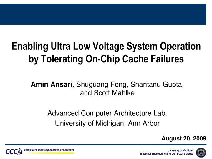
Enabling Ultra Low Voltage System Operation by Tolerating On-Chip Cache Failures Amin Ansari, Shuguang Feng, Shantanu Gupta, and Scott Mahlke Advanced Computer Architecture Lab. University of Michigan, Ann Arbor August 20, 2009 University of Michigan University of Michigan Electrical Engineering and Computer Science Electrical Engineering and Computer Science
Motivation Extreme technology integration in sub-micron regime o Heat dissipation and power density Cost of thermal packaging, cooling, and electricity Device lifetime If high performance is not needed DVS o Improvement in battery life of medical devices, laptops, and etc Large SRAM structures limit the min achievable Vdd o because SRAM delay increases at a higher rate than CMOS logic delay as Vdd is decreased University of Michigan University of Michigan 2 Electrical Engineering and Computer Science Electrical Engineering and Computer Science
Bit-Error-Rate for an SRAM Cell Extremely fast growth in failure rate with decreasing Vdd Due to systematic and random process variation o Min sustainable Vdd of entire cache is determined by the one SRAM bit-cell with the highest required operational voltage Min achievable Vdd for 64KB and 2MB caches o In 90nm while targeting 99% yield Write-margin of L2 cache determines the min Vdd University of Michigan University of Michigan 3 Electrical Engineering and Computer Science Electrical Engineering and Computer Science
Our Goal Enabling DVS to push core s Vdd down to o Ultra low voltage region ( < 600mV ) o While preserving correct functionality of on-chip caches Proposing a highly flexible and FT cache architecture that can efficiently tolerate these SRAM failures No gain in high power mode o Minimizing our overheads in this mode o Single power supply, because dual Vdd have Area and design complexity Necessity of voltage converters Large noise from the high voltage island University of Michigan University of Michigan 4 Electrical Engineering and Computer Science Electrical Engineering and Computer Science
Our Fault-Tolerant Cache Interweaving a set of n+1 partially functional cache word- lines to give the appearance of n functional lines Partitioning the set of all lines into large groups o One line per group serves as redundancy for other lines o Each line is divided to multiple chunks (smaller redundancy units) o Two lines have collision, if they have at least one faulty chunk in the same position (10 and 15 are collision free) We form groups such that there are no collision between any two lines within a group o Group 3 (G3) contains lines 4, 10, and 15 University of Michigan University of Michigan 5 Electrical Engineering and Computer Science Electrical Engineering and Computer Science
Architecture Added modules: + Memory map + Fault map + MUXing layer Group address of data line Fault map address Sacrificial line Memory Map Data line Input Address 15 4 G3 2 First Bank Second Bank 1 2 9 10 G3(1) 3 4 11 12 G3(S) 5 6 13 14 7 8 15 16 G3(2) Fault Map Two type of lines: + data line + sacrificial line MUXing layer 1 - - 2 Functional Block G3 University of Michigan University of Michigan 6 Electrical Engineering and Computer Science Electrical Engineering and Computer Science
Group Formation 1 2 G1(S) G2(1) G2(2) G3(S) G4(1) G4(2) G4(3) G5(S) 9 10 G1(1) G2(S) G1(2) G4(S) G3(1) G3(2) D G5(1) cache fault 3 4 11 12 pattern 5 6 13 14 7 8 15 16 1 G1(S) 9 G1(1) Group 1 11 G1(2) Group 2 G2(1) G2(2) 10 G2(S) 2 3 4 G3(S) Group 13 14 G3(1) G3(2) 3 12 G4(S) Group 5 6 G4(1) G4(2) G4(3) 4 7 Group 8 G5(S) 16 G5(1) 5 University of Michigan University of Michigan 7 Electrical Engineering and Computer Science Electrical Engineering and Computer Science
Operation Modes Low power mode (Vdd < 651mV) o First time processor switches to this mode BIST scans cache for potential faulty cells Processor switches back to high power mode Forms groups and fills the memory and fault maps High power mode (Vdd 651mV) o Our scheme is turned off to minimize overheads There is no sacrificial lines in this case Clock gating to reduce dynamic power of SRAM structures Bypass MUXes still burn dynamic power No power gating is used for leakage mitigation University of Michigan University of Michigan 8 Electrical Engineering and Computer Science Electrical Engineering and Computer Science
Evaluation Methodology Performance o SimAlpha that is based on SimpleScalar OoO o Processor is modeled after DEC EV-7 Delay, power and area o CACTI for caches and other SRAM structures o Synopsys standard tool-chain for Miscellaneous logic (e.g. bypass MUXes and comparators) Given set of cache parameters (e.g. Vdd) o Monte Carlo (with 1000 iterations) using described algorithm o Determining disabled portion of caches (for 99% yield) University of Michigan University of Michigan 9 Electrical Engineering and Computer Science Electrical Engineering and Computer Science
Minimum Achievable Vdd Protecting L2 is harder than L1 o Due to longer lines and larger size o Chunk size = 8b for L2 and 4b for L1 o Achieving 420mVby enforcing the following 10% limits University of Michigan University of Michigan 10 Electrical Engineering and Computer Science Electrical Engineering and Computer Science
Overheads Overheads for L1 and L2 caches o 10T used to protect fault map, tag array, and memory map Using SPEC2K benchmark suite o INT: (gzip, vpr, gcc, mcf, crafty, parser, vortex, bzip2, twolf) o FP: (swim, mgrid, applu, art, equake, ammp, sixtrack) o 4.7% performancepenalty for EV-7 (simAlpha) University of Michigan University of Michigan 11 Electrical Engineering and Computer Science Electrical Engineering and Computer Science
Conclusion DVS is widely used to deal with high power dissipation o Minimum achievable voltage is bounded by SRAM structures We proposed a flexible FT cache architecture o To tolerate these SRAM failures efficiently when operating in low power mode Using our approach o Operational voltage of processor can be reduced to 420mV o 80% dynamic power saving and 73% leakage power saving o 4.7% performance overhead for microprocessor o < 15% overhead for on-chip caches University of Michigan University of Michigan 12 Electrical Engineering and Computer Science Electrical Engineering and Computer Science