Extrinsic Semiconductors in Electronic Physics
Discover how the addition of specific dopants transforms semiconductors into n-type and p-type extrinsic semiconductors, influencing their electrical properties and enabling the creation of various semiconductor devices.

Download Presentation

Please find below an Image/Link to download the presentation.
The content on the website is provided AS IS for your information and personal use only. It may not be sold, licensed, or shared on other websites without obtaining consent from the author. If you encounter any issues during the download, it is possible that the publisher has removed the file from their server.
You are allowed to download the files provided on this website for personal or commercial use, subject to the condition that they are used lawfully. All files are the property of their respective owners.
The content on the website is provided AS IS for your information and personal use only. It may not be sold, licensed, or shared on other websites without obtaining consent from the author.
E N D
Presentation Transcript
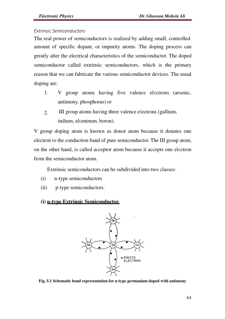
Electronic Physics Dr. Ghusoon Mohsin Ali ExtrinsicSemiconductors The real power of semiconductors is realized by adding small, controlled amount of specific dopant, or impurity atoms. The doping process can greatly alter the electrical characteristics of the semiconductor. The doped semiconductor called extrinsic semiconductors, which is the primary reason that we can fabricate the various semiconductor devices. The usual doping are: 1. V group atoms having five valence electrons (arsenic, antimony, phosphorus) or III group atoms having three valence electrons (gallium, 2. indium, aluminum, boron). V group doping atom is known as donor atom because it donates one electron to the conduction band of pure semiconductor. The III group atom, on the other hand, is called acceptor atom because it accepts one electron from the semiconductor atom. Extrinsic semiconductors can be subdivided into two classes: (i) n-type semiconductors (ii) p-type semiconductors. (i) n-type Extrinsic Semiconductor. Fig. 5.1 Schematic bond representation for n-type germanium doped with antimony 64
Electronic Physics Dr. Ghusoon Mohsin Ali This n-type is obtained when a V Group material like antimony (Sb) is added to pure semiconductor crystal; each antimony atom forms covalent bonds with the surrounding four germanium atoms with four of its five electrons. The fifth electron is loosely bound to the antimony atom. Hence, it can be easily excited from the valence band to the conduction band, practically every antimony atom introduced one conduction electron without creating a positive hole, and makes the pure semiconductor an n-type (n for negative) extrinsic. In terms of energy levels, the fifth antimony electron has an energy level (called donor level) just below the conduction band. Usually, the donor level is 0.01 eV below conduction band for germanium and 0.054 eV for silicon. In n-type semiconductor, electrons are the majority carriers (nn) while holes the minority carriers (pn), (nn) >>( pn). Fig. 5.2 The energy band diagram showing the discrete donor energy state E E N(E) f(E,T) N(E) Ec Ec Electrons EF Ev Holes N(E) N(E)(1- Fig. 5.3 The density of states function N(E), the Fermi-Dirac distribution function f(E), and areas representing electron and hole concentrations for the case when EF is above the intrinsic Fermi energy. 65
Electronic Physics Dr. Ghusoon MohsinAli (ii) p-type ExtrinsicSemiconductor. Fig. 5.4 Schematic bond representation for p-type germanium doped with boron Fig. 5.5 The energy band diagram showing the discrete acceptor energy state This p-type is obtained when a III Group material like boron (B) is added to pure semiconductor crystal. In this case, the three valence electrons of boron atom form covalent bonds with four surrounding germanium atoms but one bond is left incomplete and gives rise to a hole Thus, boron which is called an acceptor impurity causes as many positive holes in a germanium crystal as there are boron atoms thereby producing a p-type (p for positive). Accordingly, holes form the majority carriers (pp) whereas electrons form the minority carriers(np), (pp) >>(np). Fermi level shifts nearer to the valence band, the acceptor level lies immediately above the Fermi level. Conduction is by means of hole movement. 66
Electronic Physics Dr. Ghusoon MohsinAli law mass ofaction ni2=ni pi=nn pn=nppp E E N(E)f(E,T) N(E) Ec Electrons EF Holes N(E) N(E)(1-f(E,T)) Fig. 5.6 The density of states function N(E), the Fermi-Dirac distribution function f(E), and areas representing electron and hole concentrations for the case when EF is below the intrinsic Fermienergy. Majority and Minority Carriers In a piece of pure semiconductor, no free charge carriers are available at 0 K, as its temperature is raised to room temperature, some of the covalent bonds are broken by heat energy and as a result, electron-hole pairs are produced.These are called thermally-generated charge carriers/ An intrinsic semiconductor can be converted into a: p-type semiconductor by the addition of an acceptor impurity(NA) adds a large number of holes to it. Hence, in p-type holes (pp)both (NA)and (pi) added thermally-generated p = N + p p A i N-type semiconductor by the addition of an donor impurity(ND) adds a large number of electrons to it. Hence, in N-type electrons (nn) both added (ND) and n = N +n n D i 67
Electronic Physics Dr. Ghusoon MohsinAli thermally-generated (ni) Example Calculate the number of free electrons in pure silicon at ordinary temperatures. If one silicon atom out of every million atoms is replaced by an arsenic atom, how many free electrons per cubic meter are there? If density 2.33 103kg/m3, atomic weight 28.086, Eg=1.1eV. Solution n = i N N exp( Eg /2kT) =1.46 1016/m3 v c Density N N = Avo = 5 1028 /m3 Atomicweight No. of impurityatom=ND 5 1028 N = = 5 10 22 3 /m 106 D n = N + n = 5 1022+1.467 1016 n D i n = 1016 (5 106 +1.467) 5 1022 n Example Calculate the number of electrons and holes in silicon if Fermi energy is 0.25 below the conduction. At T=300K, the value of Nc=2.8 1025/m3 and Nv=1.04 1025/m3. Solution If we have the bandgap energy of silicon is 1.12 then the Fermi level will be 0.87 eV above Ev n = Nc exp( (Ec EF ) /kT) 68
Electronic Physics Dr. Ghusoon MohsinAli n =( 2.8 1025) exp( (0.25)/0.0259) =1.8 1019m 3 p = Nvexp( (EF Ev)/kT) p =( 1.04 1026) exp( (0.87)/0.0259) = 2.7 1010m 3 The change in the Fermi level is a function of the donor and acceptor impurity concentration. Compensated Semiconductor Compensated Semiconductor is one that contain both donor and acceptor impurities in the same region. During the manufacture of Semiconductor devices n-type material may have to be changed to p-type by addition acceptor impurities NA and the reverse alsorequired. If ND>>NA n-type NA>>ND p-type NA=ND intrinsic Neutrality Base: +ve charge= -ve charge p + N+= n + N D A in2 =np Andif N N n Then it isn-type N n N D A i n D A if N N n Then it isp-type A D i p N N p A D 69
Electronic Physics Dr. Ghusoon MohsinAli Example Calculate the number of electrons and holes in n-type silicon. At T=300K, if the value of ND=1022/m3 and NA=0.ni=1.5 1016/m3 Solution N N D n A i n N N 1022/m3 n D A n2 i p = n n n ( 1.5 1016) 2 p = = 2.25 1010 /m3 1022 n Example In silicon at ordinary temperatures calculate majority andminority carriers for (i) donor impurities 2.4 1019/m3 (ii) donor impurities 2.4 1019/m3 and acceptor impurities 4.8 1019/m3.Eg=1.12eV. Solution (i) in = N N exp( Eg /2kT) =1.46 1016/m3 v c majoritycarriers n = N = 2.4 1019 / m3 n D minoritycarriers ( 1.46 1016) n2 2 p =i= = 0.896 1013 /m3 2.4 1019 n n n 70
Electronic Physics Dr. Ghusoon MohsinAli (ii) p-type N N A is D NA ND ni NA ND = 2.4 1019 /m3 = 4.8 1019 2.4 1019 2.4 1019>1.46 1016/m3 p N N = 2.4 1019 /m3 p A D n2 n =i= 0.896 1013 /m3 p p p Example In silicon at ordinary temperatures calculate majority and minority carriers if doped with 3 1022/ m3acceptor impurities and 2.9 1022/m3donor impurities Eg=1.1eV. Solution Is N N D n A i N N D = 2.9 1022 3 1022 =1 1021 /m3 A ni=1.46 1016/m3 1021>>1.46 1016/m3 then pp=NA-ND=1 1021/m3 n2 n =i= 2.152 1011 /m3 p p p 71
Electronic Physics Dr. Ghusoon Mohsin Ali Problems Q1: Calculate electrons and holes concentration in a germanium sample . If T=300 K, Nd=5 1019/m3, Na=0. Assume that ni=2.4 1019/m3. (Ans: 5.97 1019/m3, 9.65 1018/m3) Q2: Calculate holes and electrons concentration in compensated silicon p-type sample. If T=300 K, Nd=3 1021/m3, Na=1022/m3. Assume that ni=1.5 1016/m3. (Ans: 7 1021/m3, 3.2 1010/m3) 72