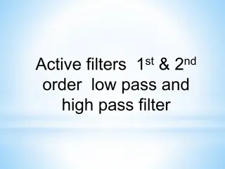
Filter Characteristics and Classifications
Explore the importance of filter characteristics in signal processing, focusing on flat frequency response and transition bands. Learn about different filter classifications based on frequency bands and circuit implementation, such as low-pass, high-pass, bandpass filters, and the distinction between passive and active implementations. Enhance your knowledge of filter design for various electronic systems.

Uploaded on | 13 Views
Download Presentation

Please find below an Image/Link to download the presentation.
The content on the website is provided AS IS for your information and personal use only. It may not be sold, licensed, or shared on other websites without obtaining consent from the author. If you encounter any issues during the download, it is possible that the publisher has removed the file from their server.
You are allowed to download the files provided on this website for personal or commercial use, subject to the condition that they are used lawfully. All files are the property of their respective owners.
The content on the website is provided AS IS for your information and personal use only. It may not be sold, licensed, or shared on other websites without obtaining consent from the author.
E N D
Presentation Transcript
General Considerations Why Filters? 2
Filter Characteristics (a) Generic and (b) ideal filter characteristics. Which characteristics of the above filter are important here? First, the filter must not affect the desired signal; i.e., it must provide a flat frequency response across the bandwidth of X(f). Second, the filter must exhibit a sharp transition [Fig(a)].More formally, we divide the frequency response of filters into three regions: the passband, the transition band, and the stopband. The characteristics of the filter in each band play a critical role in the performance. The flatness in the passband is quantified by the amount of ripple that the magnitude response exhibits. If excessively large, the ripple substantially (and undesirably) alters the frequency contents of the signal. In Fig.(b), for example, the signal frequencies between f2 and f3 are attenuated whereas those between f3 and f4 are amplified. The width of the transition band must be sufficiently narrow, i.e., the filter must provide sufficient selectivity. The stopband attenuation and ripple also impact the performance. The attenuation must be large enough below the signal level. The ripple in this case proves less critical than that in the passband, but it simply subtracts from the stopband attenuation. In Fig. (b), for example, the stopband attenuation is degraded between f5 and f6 as a result of the ripple. 3
Classification of Filters Filters can be categorized according to their various properties. We study a few classifications of filters. One classification of filters relates to the frequency band that they pass or reject. The example illustrated in previous slide is called a low-pass filter as it passes low-frequency signals and rejects high-frequency components. Conversely, one can envision a high-pass filter, wherein low- frequency signals are rejected (see Fig. below). High-pass filter frequency response. Some applications call for a bandpass filter, i.e., one that rejects both low- and high frequency signals and passes a band in between Fig. below illustrates such kind of filters Figure above summarizes four types of filters, including a band-reject response, which suppresses components between f1 and f2. 4
Classification of Filters (a) (b) (c ) Another classification of analog filters concerns their circuit implementation and includes continuous-time and discrete-time realizations. The former type is exemplified by the familiar RC circuit depicted in Fig. (a), where C1 exhibits a lower impedance as the frequency increases, thus attenuating high frequencies. The realization in Fig.(b) replaces R1 with a switched-capacitor network. Here, C2 is periodically switched between two nodes with voltages V1 and V2. In each cycle, C2 stores a charge of Q1 = C2 V1 while connected to V1 and Q2 = C2 V2 while tied to V2. For example, if V1 > V2, C2 absorbs charge from V1 and delivers it to V2, thus approximating a resistor. We also observe that the equivalent value of this resistor decreases as the switching is performed at a higher rate since the amount of charge delivered from V1 to V2 per unit time increases. The third classification of filters distinguishes between passive and active implementations. The former incorporates only passive devices such as resistors, capacitors, and inductors, whereas the latter also employs amplifying components such as transistors and op amps. (integrator) in Fig.(c). Active filters provide much more flexibility in the design and find wide application in many electronic systems. 5
Classification of Filters Summarization of filters Classifications. 6
Filter Transfer Function (a) First-order filter along with its frequency response, (b) addition of another RC section to sharpen the selectivity Filter applications point to the need for a sharp transition (a high selectivity) in many cases. How do we achieve a high selectivity? The simple low-pass filter of Fig. (a) exhibits a slope of only 20 dB/dec beyond the passband, thus providing only a tenfold suppression as the frequency increases by a factor of ten. We therefore postulate that cascading two such stages may sharpen the slope to 40 dB/dec, providing a suppression of 100 times for a tenfold increase in frequency [Fig. (b) above]. In other words, increasing the order of the transfer function can improve the selectivity of the filter. The selectivity, ripple, and other attributes of a filter are reflected in its transfer function, H(s) so it is important to get to know the properties and characteristics of filters arising from H(s). These will be analyzed in the following slides 7
Filter Transfer Function The selectivity, ripple, and other attributes of a filter are reflected in its transfer function, H(s): where zk and pk (real or complex) denote the zero and pole frequencies, respectively. It is common to express zk and pk as k + j k, where k represents the real part and k the imaginary part. One can then plot the poles and zeros on the complex plane. The poles of H (s) should always lie in the left half of the complex plane i.e their real parts should be negative for stability reasons . Why that? Recall that the impulse response of a system contains terms such as exp(pkt) = exp( kt) exp(j kt). If k> 0, these terms grow indefinitely with time while oscillating at a frequency of k [Fig(a)]. If k = 0, such terms still introduce oscillation at k [Fig (b)]. Thus, we require k < 0 for the system to remain stable [Fig(c)]. 8
Filter Transfer Function It is instructive to make several observations in regards to a filter transfer function(H(s)). (1) The order of the numerator, m, cannot exceed that of the denominator; otherwise, H(s) s as s 1, an unrealistic situation. (2) For a physically-realizable transfer function, complex zeros or poles must occur in conjugate pairs, e.g., z1 = 1 + j 1 and z2 = 1 -j 1. (3) If a zero is located on the j axis, z1,2 = (+, - ) j 1, then H(s) drops to zero at a sinusoidal input frequency of 1 (see Fig. below). This is because the numerator contains a product such as. other words, imaginary zeros force [Hj] to zero, thereby providing significant attenuation in their vicinity. For this reason, imaginary zeros are placed only in the stopband. which vanishes at s = j 1. In Effect of imaginary zero on the frequency response 9
Filter Transfer Function The figure (Fig. 12.3) presents the Specification of the transmission characteristics of a low-pass filter. The response of a filter that just meets specifications is also shown The transition band extends from the passband edge p to the stopband edge s. The ratio ( s l p) is usually used as a measure of the sharpness of the low-pass filter response and is called the selectivity factor. The low-pass filter is specified by four parameters: (1). The passband edge p, (2). The maximum allowed variation in passband transmission Amax, (3). The stopband edge s, (4). The minimum required stopband attenuation A min Example with Low-Pass Filter This filter has infinite attenuation (zero transmission) at two stopband frequencies: l1 and l12. The filter then must have transmission zeros at s = +j l1 and s = +j l2 . Since complex zeros occur in conjugate pairs, there must also be zeros at s = -j l1 and s =-j l2 . Thus the numerator polynomial of this filter will have the factors (s + +j l1 )(s -j l1 ) (s +j l2 )(s j l2 ), which can be written as (s2 + l12) (s2 + l22) . For s = j (physical frequencies) the numerator becomes (- 2 + l22 ) (- 2 + l12) which indeed is zero at = l1 and = l2 Continuing with the example we observe that the transmission decreases toward 0 as approaches . Thus the filter must have one or more zeros at s = . In general, the number of transmission zeros at s = is the difference between the degree of the numerator polynomial, m, and the degree of the denominator polynomial, n, of the transfer function). This is because as s approaches s = H (s) approaches am/sn-m and thus is said to have n-m zeros at s = 10
Filter Transfer Function Example of previous slide continued 11
Filter Transfer Function Example with Pass-band Filter A typical pole-zero plot for such a filter is shown in Fig. 12.6. 12
Filter Transfer Function As a third and final example, consider the low-pass filter whose transmission function is depicted in Fig. (a) above. We observe that in this case there are no finite values of at which the attenuation is infinite (zero transmission). Thus it is possible that all the transmission zeros of this filter are at s = . If this is the case, the filter transfer function takes the form Such a filter is known as an all-pole filter. Typical pole-zero locations for a fifth-order all pole low-pass filter are shown in Fig. 12.7(b). 13
Sensitivity The frequency response of analog filters naturally depends on the values of their constituent components. In the simple filter of Fig. below, for example, the -3-dB corner frequency is given by 1/(R1C1). Such dependencies lead to errors in the cut-off frequency and other parameters in two situations: (a) the value of components varies with process and temperature (in integrated circuits), or (b) the available values of components deviate from those required by the design (indiscrete implementations) We must therefore determine the change in each filter parameter in terms of a given change (tolerance) in each component value. This is accomplished by calculating the sensitivity of the filter with respect to the value deviations of its constituent components (R1,C1 in the pecific example) Let s assume i.e. that in the low-pass filter above resistor R1 experiences a (small) change of R1. Determine the error in the corner frequency, = 1/(R1C1).For small changes it holds: Since we interested in the relative (percentage) error in in terms of the relative change in R1, we have: This means for example that a +5% change in R1 translates to a -5% error in . 14
Sensitivity The example of previous slide leads to the concept of sensitivity, i.e., how sensitive each filter parameter is with respect to the value of each component. Since in the first-order circuit, we say the sensitivity of with respect to R1 is unity in this example. More formally, The sensitivity of parameter P with respect to acomponent value C is defined as: It is obvious that Sensitivities substantially higher than unity are undesirable As a last example and based on the above the calculation of the sensitivity of with respect to C1 for the low-pass filter is given as follows: We calculate the first derivative with respect to C1 and we get : and hence 15
First- Order Filters In the following, we will consider first-order realizations, described by the transfer functions: The circuit of the previous slide and its transfer function are examples of such filter types In general , first order filters and its transfer function (shown above) could lead only to low- pass or high pass-ones. Specifically, depending on the relative values of z1 and p1, low-pass or high-pass characteristics are conveyed by the specific filter results are , as illustrated in the plots of Fig. below. Note that the stopband attenuation factor is given by z1/p1 First-order (a) high-pass and (b) low-pass filters. 16
First- Order Filters Parametrized Examples The below circuit is firstly considered as a candidate for realization of the specific first order transfer function Its transfer function as can be easily derived is : The circuit therefore contains a zero at -1/(R1C2) and a pole at -1=[R1(C1 + C2)] plottedin Fig. below. Note that the zero arises from C2. It s easy to note that since z1 = -1/(R1C2 and p1= -1/[R1(C1 + C2)] , the zero always falls above the pole, allowing only the response shown in Fig. (b) of previous slide i.e. that of a low-pass filter 17
First- Order Filters Parametrized Examples The transfer function of the circuit is derived as follows: The circuit contains a zero at -1/(R1C1) and a pole at -[(C1 + C2)R1 II R2]-1. Depending on the component values, the zero may lie below or above the pole thus resulting in high pass or low pass behaviour respectively Specifically, for the zero frequency to be lower: = => or 18
First- Order Filters Active Counterpart Circuit The active counterpart of the filter in previous slide is shown in Figure below: Assuming that the gain of the op-amp is large it holds: Figure 14.18 19
Second-Order Filters The first-order filters studied above provide only a slope of -20 dB/dec in the transition band. For a sharper attenuation, we must seek circuits of higher order. The general transfer function of second-order filters is given by the biquadratic equation the denominator is expressed in terms of quantities n and Q because they signify important aspects of the response. We begin our study by calculating the pole frequencies. Since most second-order filters incorporate complex poles, we assume and As the quality factor of the poles, Q, increases, the real part decreases while the imaginary part approaches (+ - ) n-see Fig. below. In other words, for high Q s, the poles look very imaginary, thereby bringing the circuit closer to instability Variation of poles as a function of Q. 20
Second-Order Filters A few special cases of the biquadratic transfer function will be analyzed that prove useful in practice. First, suppose = = =0 so that the circuit contains only poles and operates as a low-pass filter (why?). The magnitude of the transfer function is then obtained by making the substitution s= j and we get: It can be shown that the response is (a) free from peaking if and (b) reaches a peak at (Fig. 14.20). In the latter case, In the latter case, the peak magnitude is Frequency response of second-order system for different values of Q 21
Second-Order Filters(Highpass and Bandpass characteristics) High Pass How does the bi quadrative transfer function provide a high-pass response? In a manner similar to the first-order realization, the zero(s) must fall below the poles. For example, with two zeros at the origin we get : a) Pole and zero locations and (b) frequency response of a second-order high-pass filter 22
Second-Order Filters(Highpass and Bandpass characteristics) High Pass Is it possible that a high-pass response can be obtained if the biquadratic equation contains only one zero? In such a case : It is obvious that since H(s) 0 as s , the system cannot operate as a high-pass filter. Band Pass A second-order system can also provide a band-pass response. In that case the transfer function has the following form: It can be seen that the magnitude approaches zero for both s 0 and s , reaching a maximum in between. It can be proved that the peak occurs at = n and equals to Q/ n. (a) Pole and zero locations and (b) frequency response of a second-order band-pass filter 23
Second-Order Filters(Highpass and Bandpass characteristics) Band Pass The Determination of the -3-dB bandwidth of the response of the Bandpass Filter of the previous slide is calculated as follows: As shown in Fig. below the response reaches 2, exhibiting a bandwidth of 2- 1 times its peak value at frequencies 1 and To calculate 1 and 2, we equate the squared magnitude to => The total -3-dB bandwidth spans 1 to 2 and is equal to n/Q. 24
RLC Realizations It is possible to implement the second-order transfer function by means of RLC realizations, since they (a) find practical applications in low-frequency discrete circuits or high-frequency integrated circuits, and (b) prove useful as a procedure for designing active filters. We therefore study their properties here and determine how they can yield low-pass, high-pass, and band- pass responses. Consider the parallel LC combination (called a tank ) depicted in Fig. below We get: (a) LC tank, (b) imaginary poles, and (c) frequency response 25
RLC Realizations Based on the results of LC tank we analyze now the full RLC circuit Z2 can be obtained by replacing R1 in parallel with Z1 in transfer function of The impedance still contains a zero at the origin due to the inductor. The poles are computed as follows: 26
RLC Realizations As long as the excitation of the circuit does not alter its topology, the poles are given as above, a point that proves useful in the choice of filter structures. 27
RLC Realizations Low-Pass Filter Based on the observations mentioned in previous slide it is derived that the circuit below forms an RLC type realization of an LPF filter, since This arrangement provides a low-pass response having the same poles as those given by (14.39) or (14.43) because for Vin = 0, it reduces to the topology of Fig. 14.26. furthermore, the transition beyond the passband exhibits a second-order roll-off because both It can be shown that: 29
RLC Realizations Low-Pass Filter If the Q of the network is sufficiently high, the frequency response exhibits peaking, i.e., a gain of greater than unity in a certain frequency range. The transfer function provides this effect if the denominator falls to a local minimum Comparison with the condition provided during RLC analysis in previous slides reveals that the poles are complex here. 30
Active Filters Passive filters suffer from a number of drawbacks; e.g., they constrain the type of transfer function that can be implemented, and they may require bulky inductor. For these reasons active implementations are preferred Most active filters employ op amps to allow simplifying idealizations and hence a systematic procedure for the design of the circuit. An important concern in the design of active filters stems from the number of op amps required as it determines the power dissipation and even cost of the circuit. In the following second order realizations will be considered using one, two, or three op amps. Sallen and Key Filter The low-pass Sallen and Key (SK) filter employs one op amp to provide a second-order transfer function (see Fig. below). Note that the op amp simply serves as a unity-gain buffer, Basic Sallen and Key Filter. Assuming an ideal op amp, we have VX = Vout. Also, since the op amp draws no current, the current flowing through R2 is equal to VXC2s = VoutC2s, Note: Please note that in the following slides regarding Salien and Key filters, n might also be mentioned as 33
Active Filters Sallen and Key Filter-LPF case As mentioned in previous slide , we have VX = Vout, while also since the op amp draws no current, the current flowing through R2 is equal to VXC2s = VoutC2s, yielding Forming a KCL at node Y gives and after some calculations: To obtain a form similar to that (with = =0) we divide the numerator and the denominator by R1R2C1C2 and define 34
Active Filters Sallen and Key LPF filter-Graphical representations for various Q and The frequency o is referred to as the cutoff frequency of the filter, although the exact value of the cutoff frequency,, is equal to o only for Q = 1/ 2. At low frequencies that is, << o the filter has unity gain, but for frequencies well above o, the filter response exhibits a two- pole roll-off, falling at a rate of 40 dB/decade. At = o, the gain of the filter is equal to Q LPF response for o = 1 and four values of Q. Figure above shows the response of the filter for o = 1 and four values of Q: 0.25, 1/ 2, 2 and 10. Q = 1/ 2 corresponds to the maximally flat magnitude response of a Butterworth filter, which gives the maximum bandwidth without a peaked response. For a Q larger than 1/ 2, the filter response exhibits a peaked response that is usually undesirable, whereas a Q below 1/ 2 does not take maximum advantage of the filter s bandwidth capability. From a practical point of view, a much wider selection of resistor values than capacitor values exists, and the filters are often designed with C1 = C2 = C. Then o and Q are adjusted by choosing different values of R1 and R2. For the equal capacitor design 35
Active Filters Sallen and Key LPF filter with gain>1 The SK topology below can provide a passband voltage gain of greater than unity for an LPF. Specifically we note that (1 + R3/R4)VX = Vout , and the current flowing through R2 is given by VXC2s = VoutC2s/(1 + R3/R4). It follows that Vy equals to: Forming a KCL at node Y yields And solving for Vout we get: 36 It is interesting here to note that n remains the same
Active Filters Sallen and Key LPF filter with gain>1, Sensitivity Issues An important objective in choosing the values in filters is to minimize the sensitivities of the circuit. Considering the topology shown in previous slide and defining K = 1+R3/R4 we compute the sensitivity of n and Q with respect to the resistor and capacitor values we have that and hence: 37
Active Filters Sallen and Key LPF filter with gain>1, Sensitivity Issues For the Q sensitivities, we first rewrite Eq. in terms of K = 1+R3/R4: (14.80) 38
Active Filters Sallen and Key LPF filter with gain>1, Sensitivity Issues In applications requiring a high Q and/or a high K, one can choose unequal resistors or capacitors so as to maintain reasonable sensitivities. As an example, let s assume that an SK filter must be designed for Q = 2 and K = 2. Determine the choice of filter components for minimum sensitivities 39
Active Filters Sallen and Key LPF filter with gain>1, Sensitivity Issues 40
Active Filters A high-pass filter can be achieved with the same topology as that of LPF by interchanging the position of the resistors and capacitors, as shown in specific Figure. Also the voltage follower in the low-pass filter has been replaced with a noninverting amplifier with a gain of K. Gain K provides an additional degree of freedom in the filter design. The analysis is similar to that of LPF Sallen and Key filter - High Pass case It holds that: V2= Vo R/[(k-1)R +R]=> Vo= KV2, ic2= V2 /R2= Vo / KR2 V1= VC2+V2= ic2/ sC2 + Vo / K = Vo / K (1 /R2sC2 +1)= Vo / K [ (1 +R2sC2 )/R2 sC2)] Using KCL at node V1, we have: iC1 + iR1 +iC2=0 where: : iC1 = (V1- Vin)/ Zc1 = (V1- Vin) sC1 => iC1 = [ [Vo / K [ (1 +R2sC2 )/R2sC2)] - Vin] sC1, ic2= Vo / KR2 and iR1 = (V1- Vo)/ R1 = [ [Vo / K [ (1 + R2sC2 )/ R2sC2)] - Vo] / R1 . Substituting the expressions for : iC1 , iR1 , iC2 to the KCL equation and after some calculations we have: with or , 41
Active Filters Sallen and Key High Pass filter-Graphical representations for various Q and values Figure in the left shows the high-pass filter responses for a filter with o = 1 and four values of Q. The parameter o corresponds approximately to the lower-cutoff frequency of the filter, and Q = 1/ 2 again represents the maximally flat, or Butterworth, filter response. Usually the case R1 = R2 = R and C1 = C2 = C is used for this filter design, where H(s), and Q are simplified to HPF response for o = 1 and 4 Q values. The noninverting amplifier circuit obviously must have K 1. Note that K = 3 for this case corresponds to infinite Q. This situation corresponds to the poles of the filter being exactly on the imaginary axis at s = j o and results in sinusoidal oscillation. For K > 3, the filter poles will be in the right-half plane, and thus values of K 3 correspond to unstable filters. Therefore, 1 K < 3. 42
Active Filters Sallen and Key filter - Band pass case A band-pass filter can be realized by combining the low-pass and high-pass characteristics of the corresponding filters. Figure below shows one possible circuit for such a band-pass filter. (a) Band-pass filter using inverting op amp (b) Simplified band-pass filter after Thevenin is applied It holds: ic2=(V1-0)/Zc2 = V1/ (1/sC2 )= sV1C2 , iR2= [(Vo -0)/R2], ic2= - iR2 => sV1C2 = - Vo /R2 => V1 = - Vo /s C2R2 Using KCL at node V1, we have: iRth + ic1 +ic2=0=> - iRth =ic1 +ic2 => - ( 1 -Vth )/Rth= ic1 +ic2 . Setting Gth =1/ Rth we get : Combining the above equation with the expression derived for V1 we have: Finally substituting Vthwith the equivalent expression with Vin we get 43
Active Filters Sallen and Key BandPass filter-Graphical representations for various Q and values The response of the band-pass filter is shown in Figure on the left for o = 1, C1 = C2, R3 = , and three values of Q. Parameter o now represents the center frequency of the band-pass filter. The response peaks at o, and the gain at the center frequency is equal to 2Q2. At frequencies much less than or much greater than o, the filter response corresponds to a single- pole high- or low-pass filter, changing at a rate of 20 dB/decade. A usual design choice for this filter is to have C1 set equal to C2 = C, where the expressions for H(s), and Q become: 44
Integrator-Based Biquads KHN biquad Filters It is possible to realize the biquadratic transfer function by means of integrators. Let us consider a special case where = = 0, i.e.a High Pass Filter This expression suggests that Vout can be created as the sum of three terms: a scaled version of the input, an integrated version of the output, and a doubly-integrated version of the output. Figure below illustrates how Vout is generated by means of two integrators and a voltage adder (a) Flow diagram showing the generation of Vout as a weighted sum of three terms 45
Integrator-Based Biquads The corresponding circuit realization is depicted in Fig. below. b) realization of KHN filter, Note that the inherent signal inversion in each integrator necessitates returning VX to the noninverting input of the adder and VY to the inverting input. It holds that: (c) simplified diagram for calculating Vout we obtain from Fig. (c) the weighted sum of Vin, VX , and VY as Equating similar terms in eq .above and we get 46 It is thus possible to select the component values so as to obtain a desired transfer function.
Integrator-Based Biquads LPF and BPF filters The topology of Figure (on the left) is called the KHN biquad after its inventors, Kerwin, Huelsman, and Newcomb. This topology proves quite versatile, since in addition to providing the high-pass transfer function of previous slide the circuit can also serve as a low-pass and a band-pass filter. Specifically, BPF case If in the above Figure the output is taken from X then we have a Band pass filter since which is a bandpass transfer function LPFcase If in the above Figure the output is taken from Y then we have a Lowpass filter since which is a lowpass transfer function The most important attribute of the KHN biquad is its low sensitivities to component values. It can be shown that the sensitivity of n with respect to all values is equal to 0.5 and It is Interesting to note that, if R3 = R6, then SQR3;R6 vanishes The use of three op amps in the feedback loop of Fig. above raises concern regarding the stability of the circuit because each op amp contributes several poles. Careful simulations are necessary to avoid oscillation. 47
Integrator-Based Biquads Another type of biquad developed by Tow and Thomas is shown in Fig. on the left Here, the adder and the first integrator are merged, and resistor R3 is introduced. (Without R3, the loop consisting of two ideal integrators oscillates.) Noting that VX = -VY and Tow and Thomas Biquad Filters , we sum the currents flowing through R4 and R1 and multiply the result by the parallel impedances of R3 and C1 => which provides a band-pass response The output at Y exhibits a low-pass behavior It can be shown that the sensitivities of the Tow-Thomas biquad with respect to the componentvalues are equal to 0.5 or 1 48
Biquads Using Simulated Inductors In previous slides it was shown that second- order RLC circuits can provide low-pass, high- pass, or band-pass responses, but their usage in integrated circuits is limited because of the difficulty in building high-value, high-quality on-chip inductors. We may therefore ask: is it possible to emulate the behavior of an inductor by means of an active (inductorless) circuit? The answer is given by the circuit on the left General impedance converter Consider the circuit shown in Fig. above, where general impedances Z1-Z5 are placed in series and the feedback loops provided by the two (ideal) op amps force V1-V3 and V3- V5 to zero: V1 = V3 = V5 = VX That is, the op amps establish a current of VX/Z5 through Z5. This current flows through Z4, yielding V4 =(VX/Z5)Z4 + VX: The current flowing through Z3 (and hence through Z2) is given by: IZ3= (V4 -V3)/Z3=(VX/Z5 ) (Z4/Z3): The voltage at node 2 is thus equal to: V2 = V3 - Z2 IZ3 = VX - Z2 (VX/Z5 ) (Z4/Z3): Finally, IX= (VX -V2)/ Z1 = VX ( Z2 Z4)/ (Z1 Z3 Z5) and hence : 49
Biquads Using Simulated Inductors The result derived in previous slide, i.e. suggests that the circuit can convert Z5 to a different type of impedance if Z1 - Z4 are chosen properly. For example, if Z5 = RX, Z2 = (Cs)-1, and Z1 = Z3 = Z4 = RY we can get from the Figure below that: which is an inductor of value RX RY C. We say the circuit converts a resistor to an inductor, i.e., it simulates an inductor. Example of inductance simulation. From Eq. above, another possible combination of components that yields a simulated inductor is to choose Z4 = (Cs)-1 and the remaining passive elements to be resistors: Z1 =Z2 = Z3 = RY . Thus, by the Eq. above it is derived that: Zin = RX RY C s The resulting topology is shown in Fig. on the left 50


")
")
")