Frequency Response Analysis of Common Gate (CG) Stage Circuits
Explore the frequency response and noise contributions of Common Gate (CG) stage circuits in microelectronic system design. Understand the small signal circuit hypotheses, current division between components, and typical cases affecting the performance. Gain insights into the impact of parasitic capacitances, signal sources, and transconductance parameters on circuit behavior.

Download Presentation

Please find below an Image/Link to download the presentation.
The content on the website is provided AS IS for your information and personal use only. It may not be sold, licensed, or shared on other websites without obtaining consent from the author. If you encounter any issues during the download, it is possible that the publisher has removed the file from their server.
You are allowed to download the files provided on this website for personal or commercial use, subject to the condition that they are used lawfully. All files are the property of their respective owners.
The content on the website is provided AS IS for your information and personal use only. It may not be sold, licensed, or shared on other websites without obtaining consent from the author.
E N D
Presentation Transcript
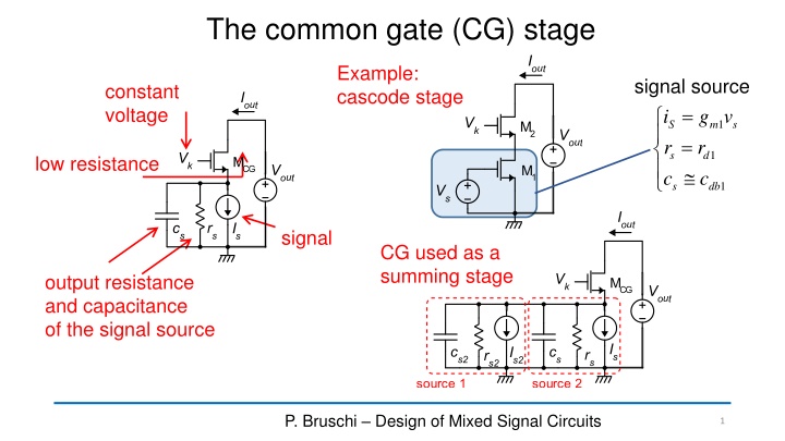
The common gate (CG) stage Example: cascode stage signal source constant voltage = = i r c g v r c 1 S m s 1 s d low resistance 1 s db signal CG used as a summing stage output resistance and capacitance of the signal source P. Bruschi Design of Mixed Signal Circuits 1
Frequency response of the common gate stage Hypothesis: Vkis at gnd in the small signal circuit. For example, it is provided by an ideal voltage source small-signal circuit with parasitic capacitances = + + c c bs cg c c gs cg p s P. Bruschi Microelectronic System Design 2
Frequency response of the common gate stage 1 z = = s i out i i 1 1 s s current division between Rinand zs + + 1 z s g g z m cg m cg s 1 z 1 r = + sc 1 p = out i i s s s 1 1 r + + 1 sc p g m cg s 1 = out i i s sc g 1 p + + 1 1 + 1 = R g r in m cg s m cg g g g mb cg m cg m cg P. Bruschi Microelectronic System Design 3
Frequency response of the common gate stage ( ) 0 I CG A 1 1 1 out i i = out i i ( ) = = A s s sc g 1 1 I 1 p + + 1 c + 1 1 s p + + g r 1 1 s g r m cg s m cg g g r m cg s m cg m cg s 1 ( ) s ( ) 0 1 = I CG A I CG A 1 r g r Typical case: s m cg s s + g 1 m cg p 1 ( ) 0 g = 1 I CG A m cg c 1 p + 1 p g r m cg s P. Bruschi Microelectronic System Design 4
Frequency response of the common gate stage g m cg c p p In many cases, the main contribution to cpis the cgs of the CG MOSFET g c m cg f T CG p gs cg P. Bruschi Microelectronic System Design 5
Noise contribution of a CG stage zs=cp//rs Every time we have a floating current source, we can split it into two sources with one terminal at ground n cg i n cg i = = n cg i P. Bruschi Microelectronic System Design 6
Noise contribution of a CG stage in-out ( ) ( ) = n cg i 1 n cg i A s = A s n out i n cg i I I n cg i n cg i n cg i = = n cg i MCG g + r 1 ( ) 0 zs m cg s g = = = A I CG A In DC: n cg i 1 I 1 r + 1 m cg s g r m cg s g + r 1 n out i i 1 ( ) 0 m cg s g = = 1 1 A + + 1 g r 1 1 r g r m cg s n cg m cg s m cg s P. Bruschi Microelectronic System Design 7
Summary of properties of a CG stage in typical cases 1 s m cg g g r g r + g c 1 r g r m cg s ( ) 0 1. m cg s = 1 I CG A 1 m cg s m cg 2. p p n out i i ( ) = 1 A j p = 3. f f This factor is << 1 for p 2 n cg 1 1 n out i i = 1 In DC: + 1 g r g r m cg s m cg s n cg P. Bruschi Microelectronic System Design 8
 stage")