Graphene, a 2-D carbon sheet with unique properties, holds immense potential in various fields. This presentation outlines its structure, electrical and thermal properties, market status, and future in semiconductors. Despite challenges, graphene is a promising material with significant implications.
Please find below an Image/Link to download the presentation.
The content on the website is provided AS IS for your information and personal use only. It may not be sold, licensed, or shared on other websites without obtaining consent from the author. If you encounter any issues during the download, it is possible that the publisher has removed the file from their server.
You are allowed to download the files provided on this website for personal or commercial use, subject to the condition that they are used lawfully. All files are the property of their respective owners.
The content on the website is provided AS IS for your information and personal use only. It may not be sold, licensed, or shared on other websites without obtaining consent from the author.
Presentation Outline Graphene structure and Properties Graphene in the marketplace Fabrication and production Uses in electronics Experimental Uses Summary
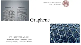
Graphene Structure Graphene is a 2-D, one atom thick sheet of carbon.This shape forms the foundation of other atomic structures like carbon nanotubes. Strength of the structure comes from numerous double bonds interspersed throughout the honeycomb structure.
Electrical and Thermal Properties Electrons in graphene move extremely easily, passing over the bandgap with little effort, electrons in graphene are known as massless electrons due to this property Graphene is extremely thermally conductive. Transparent, only absorbs 2% of light that passes through it Possibly hazardous to breathe or ingest, irritant to skin and eyes
Graphene in the Market Despite widespread experimentation of graphene in several fields, it has yet to catch on commercially. Most Commercial uses involve composite materials used in sports equipment such as bike chassis, tennis rackets, and helmets. Commercial electrical applications include heat sinks for computer components and biosensors for medical devices.
Graphene In Semiconductors Although graphene is currently difficult to manufacture, it s main component, graphite is very abundant Graphene is poised to replace indium tin oxide and other thin film semiconductor materials in the near future as a more durable and sustainable alternative Conductive properties of graphene yield a very high mobility and the material s thermal conductivity may allow it to handle higher frequency operation than silicon devices
Challenges to Graphene as a Semiconductor Manufacturing difficulties make graphene expensive. This issue will be mitigated over time as the market grows and as new technologies emerge. The lack of a bandgap in graphene will make it more difficult to replace silicon in transistors Logistically, it will take time for graphene to both become less expensive and more available relative to other commonly used materials today.
ISO Classifications for Graphene Graphene Monolayer: A single Layer of graphene Graphene Bilayer: Two well defined stacked graphene layers Few-layer Graphene: 3-10 well defined stacked graphene layers Graphene nanoplatelet: Undefined number of layers between 1-3nm thick. This classification makes up about 90% of graphene today. Graphite: 3D structure that is thicker than 3nm. Graphene oxide (GO): Typically produced through exfoliation. Reduced Graphene Oxide (RGO): Produced from GO in a Number of ways. Becomes Graphene when fully reduced.
Fabrication Methods: Mechanical Exfoliation Mechanical Exfoliation: Pulling or cleaving layers of graphite apart to make graphene. These methods include the original scotch tape method, cleaving graphite with a single crystal diamond wedge, and slow speed ball milling. Mechanical methods Often provide, defect free and unoxidized graphene. Though it is often slower than other methods
Fabrication Methods: Ultrasonic Exfoliation Ultrasonic Exfoliation: Graphite is submerged in a liquid and blasted with sound at a frequency above 20Khz. Liquid mediums vary, although ionic fluids have the strongest yield. Graphene flakes have a higher chance to restack with this method. This can be combated through the use of a surfactant solvent, although this requires the graphene to go through additional chemical treatment to remove the surfactant.
Fabrication Methods: Chemical Vapor Deposition The CVD method of producing graphene entails using copper as a substrate to grow graphene on. Heated methane deposits its carbon atoms on the copper in a monolayer. To prevent graphene from sticking to the copper, a thin parylene sheet is used as a buffer. This method allows for the production of large sheets of graphene.
The Bandgap in Graphene It s difficult to create a bandgap in graphene while maintaining its excellent conductive properties Methods of physically engineering graphene with a bandgap are more successful at preserving the valuable characteristics; Straining, Corrugating and Coupling to hexagonal or metal substrates (h-BN) Methods of chemically engineering graphene with a bandgap are more likely to change the lattice in a way removes its valuable properties, but most likely to be used commercially due to high volume potential; hydrogenation, fluorination, and doping
Graphene in Radio Frequency Transistors Estimated values for cutoff frequency and maximum oscillating frequency in graphene transistors are much higher than silicon, estimated device parameters also suggest much higher mobility and contact resistance than silicon. In experimental devices, it was observed that mechanically exfoliated graphene experienced impurities that increased contact resistance and decreased mobility. Poor interaction between graphene and commonly used metals is to blame for poor contact resistance.
GFETs GFETs or graphene based field effect transistors have several designs with graphene as the channel with metal electrodes and graphene as electrodes. Graphene nano ribbon (monolayer and 10 nm wide) was found to act as an effective channel Typically fabricated on Si/SiO2 substrates Extremely high sensitivity and very good surface area to volume ratio GFETs are typically used as extremely sensitive sensors and biosensors Biosensors are devices that detect the presence or concentration of a biological structure.
Graphene in Solar Cells Graphene s unique combination of transparency, conductivity and flexibility make it ideal for use in modern solar cells Sheet resistance of graphene was initially higher than expected. As with other applications, finding methods of altering graphene to be more usable while also retaining valuable electric properties proved difficult. In experimental trials CVD fabricated graphene that was then subjected to a complicated doping process that resulted in p-doped functionalities that reduced sheet resistance to tolerable levels while retaining necessary transparency and mobility.
Summary Graphene is a unique material whose physical and chemical properties are still being explored Graphene will have a large impact on the development of modern technology, being that it is a young technology, we are still years away from its full potential Overcoming hurdles to become a promising semiconductor material Manufacturing techniques are advancing allowing for graphene to be specialized for more applications From transistors to paint, graphene has applications everywhere
Topics For Questions What areas does graphene perform poorly in device design compared to traditional semiconductors? How do the properties of graphene change when compared to monolayer, bilayer, and flake graphene? Why does graphene interact poorly with metals and some substrate materials? What essential properties of semiconductors suffer from these interactions? Graphene can be fabricated in a variety of methods, which is most likely to see widespread commercial use?