High Electron Mobility Transistors (HEMTs)
"Discover the history, structure, and applications of High Electron Mobility Transistors (HEMTs), which operate in the microwave range and utilize a 2-dimensional electron gas for enhanced performance. Learn about the differences from MOSFETs, fabrication techniques, and how HEMTs work."

Uploaded on | 3 Views
Download Presentation

Please find below an Image/Link to download the presentation.
The content on the website is provided AS IS for your information and personal use only. It may not be sold, licensed, or shared on other websites without obtaining consent from the author. If you encounter any issues during the download, it is possible that the publisher has removed the file from their server.
You are allowed to download the files provided on this website for personal or commercial use, subject to the condition that they are used lawfully. All files are the property of their respective owners.
The content on the website is provided AS IS for your information and personal use only. It may not be sold, licensed, or shared on other websites without obtaining consent from the author.
E N D
Presentation Transcript
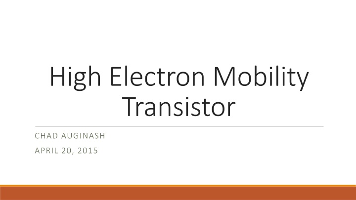
High Electron Mobility Transistor CHAD AUGINASH APRIL 20, 2015
Abstract High electron mobility transistor(HEMT) is a transistor that operates at higher frequencies, typically in the microwave range. They are used in applications that require high frequency, such as cell phones, RF applications, and some power applications. HEMTs are transistors that utilize the 2-dimensional electron gas(2DEG) created by a junction between two materials with different band gaps called a heterojunction. The two most commonly used materials to create the heterojunction are a highly doped n-type donor material, typically AlGaAs and an undoped material, typically GaAs.
Outline History Specific HEMT example Differences between MOSFETs and HEMTs Applications Summary How HEMTs work? Structure
History The invention of the HEMT is credited to Takashi Mimura in 1979. Mimura couldn t build the HEMT until he heard about a modulation-doping technique developed at Bell Laboratories Dingle et al. at Bell laboratories developed the modulation-doped heterojunction superlattice, which was instrumental in the development of the HEMT In 1986, a telescope equipped with a HEMT amplifier discovered new interstellar molecules in the Taurus Molecular Cloud about 400 light years away
Differences between MOSFETs and HEMTs HEMTs MOSFETs Operation in the UHF range (300MHZ-3Ghz) Operate in the microwave range (300MHZ-300GHz) Heterojunction is used as the channel Doped region is used as the channel
How do HEMTs work? HEMT s take advantage of 2DEG which is created at the AlGaAs/GaAs heterojunction. The 2DEG is confined at the heterojunction and free to move parallel to the channel. This results in a higher electron mobility which is good for large gain and high frequency characteristics. Fig1.Energy band diagram for AlGaAs/GaAs heterojunction at thermal equilibrium
Fabrication Molecular beam epitaxy(MBE) is one of the growth techniques used to create the AlGaAs/GaAs heterojunction Metal organic chemical vapour deposition(MOCVD) is another common process used to create the heterojunction Fig 2. SEM image of a cross-section structure of alternating 500nm layers of GaAs and AlGaAs Other typical lift-off techniques are used to create the contacts
Molecular beam epitaxy(MBE) Materials are grown using MBE are grown in a low pressure vacuum usually down to 10 11 torr Effusion cells are used to direct the material onto the substrate. Effusion is where individual molecules travel through a small hole without collision. Effusion cells are turned off and on by shutters and controlled by the temperature of the cell. Fig 3. Diagram showing the main components and rough layout of the main chamber of the MBE system
Reflection high energy electron diffraction(RHEED) RHEED is an in-situ characterization tool used in the MBE process RHEED can relay information to the user about the surface structure, roughness, growth rate, and cleanliness RHEED allows high levels of accuracy in the thickness of the material grown Fig 4. Diagram showing the main components and rough layout of the main chamber of the MBE system
Structure Typical cross sectional view of a GaN HEMT Structure is similar for GaAs The lattice matching layer is used to match the different lattice structures of the GaN and the Si substrate. Lattice matching is important for the electron mobility GaN has been grown on sapphire because of the superior lattice structure matching Fig 5. GaN HEMT structure
Fujitsus InP HEMT InP HEMTs exhibit a current-gain cutoff frequency of 500Ghz making them the fastest transistors to date (2006) Fujitsu introduces a Y-shaped structure for the gate. The large cross sectional of the gate electrode is used to reduce gate resistance. The small gate contact is used to reduce gate length Fig 6. Cross sectional view of the InP HEMT
Fujitsus cavity structure in the InP HEMT Fujitsu s cavity structure reduces gate electrode parasitic capacitance Increased capacitance between gate and drain is almost zero Capacitance between gate and source is nearly halved The reduction is parasitic capacitance leads to a 14% increase in speed in a static frequency divider Fig 7. Cavity structure in InP HEMT
Materials used in HEMTs GaAs: used in the first HEMTs GaN: an improvement upon the GaAs based HEMTs InP: used in some of the most advanced HEMTs today
Applications Precision sensors Next generation wired/wireless communication Advanced radars Power electronics
Passive millimeter wave image sensor Millimeter wave image sensors are used at TSA checkpoints Passive device that detects electromagnetic waves radiation Millimeter waves can pass through clothing, fire, and thin walls, to detect a human body, making it ideal for security and disaster prevention. Fig 8. Block diagram of passive imaging sensor
Passive millimeter wave image sensor Low noise amplifier(LNA) used in the passive millimeter wave image sensor Millimeter wave image sensor is limited to short range due to atmospheric attenuation Frequencies at 94Ghz, 140GHz, and 220GHz have relatively low atmospheric attenuation 94GHz band is used for this particular millimeter wave image sensor Fig 9. Electrical performance of LNA using InP HEMTs Fig 10. Millimeter wave image of human body
Summary Reliability of GaN and InP HEMT s are excellent at lower frequencies Reliability issues need to be resolved in Gan and InP HEMT s at higher frequencies Failure mechanisms such as gate sinking, thermal degradation of ohmic contact, and charge trapping needs further investigation New structures need to be developed to reduce parasitic capacitance and address the failure mechanisms
References Cho, A. Y., and J. R. Arthur. "Molecular beam epitaxy." Progress in solid state chemistry 10 (1975): 157-191. Dingle, R., et al. "Electron mobilities in modulation doped semiconductor heterojunction superlattices." Applied Physics Letters 33.7 (1978): 665- 667. Kawano, V. Yasuhiro Nakasha V. Yoichi, V. Masaru Sato, and V. Tsuyoshi Takahashi V. Kiyoshi Hamaguchi. "Ultra high-speed and ultra low-noise InP HEMTs." Fujitsu Sci. Tech. J 43.4 (2007): 486-494. Khan, M. Asif, et al. "High electron mobility transistor based on a GaN AlxGa1 xN heterojunction." Applied Physics Letters 63.9 (1993): 1214-1215. Meneghesso, Gaudenzio, et al. "Reliability of GaN high-electron-mobility transistors: state of the art and perspectives." Device and Materials Reliability, IEEE Transactions on 8.2 (2008): 332-343. Mimura, Takashi. "The early history of the high electron mobility transistor (HEMT)." IEEE Transactions on microwave theory and techniques 50.3 (2002): 780-782. Neamen, Donald A. "Semiconductor physics and devices." 1992 (1994). http://en.wikipedia.org/wiki/High-electron-mobility_transistor http://en.wikipedia.org/wiki/Molecular_beam_epitaxy
Concepts 1. Who is credited with inventing the HEMT? 2. What material was first to create the HEMT? 3. Name two applications for HEMT. 4. Name two materials used in HEMT. 5. What is used as the channel in the HEMT?


")