HIGH ELECTRON MOBILITY TRANSISTORS
HEMTs, incorporating a junction between materials with different band gaps, are discussed along with various types like GaN HEMT and InP HEMT. Explore design rules, applications, and a comparison with GaAs HEMT for technology advancements.

Download Presentation

Please find below an Image/Link to download the presentation.
The content on the website is provided AS IS for your information and personal use only. It may not be sold, licensed, or shared on other websites without obtaining consent from the author.If you encounter any issues during the download, it is possible that the publisher has removed the file from their server.
You are allowed to download the files provided on this website for personal or commercial use, subject to the condition that they are used lawfully. All files are the property of their respective owners.
The content on the website is provided AS IS for your information and personal use only. It may not be sold, licensed, or shared on other websites without obtaining consent from the author.
E N D
Presentation Transcript
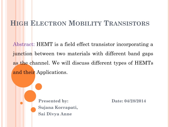
HIGH ELECTRON MOBILITY TRANSISTORS Abstract: HEMT is a field effect transistor incorporating a junction between two materials with different band gaps as the channel. We will discuss different types of HEMTs and their Applications. Presented by: Date: 04/28/2014 Sujana Korrapati, Sai Divya Anne
OUTLINE Introduction GaN HEMT structure and operation principles Design rules for AlGaN/GaN HEMT InP HEMT Comparison of GaN HEMT with GaAs HEMT Applications in Technology Summary
INTRODUCTION Transistors are used in electronic devices e.g. switch, amplifiers, oscillators To satisfy the growing demands of High Power High Speed High Efficiency communications Conventional HEMTs use a AlGaAs/GaAs AlGaN/GaN
BASIC GAN HEMT STRUCTURE Source: http://www.eetimes.com/document.asp?doc_id=1272514
GALLIUM NITRATE High electron density(Polarization effects) Adequate for high power amplifiers High Breakdown voltage Large heat capacity Necessary to growth in a wafer of another material Molecular Beam Epitaxy Metal Organic Vapor Beam Epitaxy
SUBSTRATE MATERIAL Sapphire Most used material, cheap, good quality commercial wafers. Poor thermal conductivity. Silicon Carbide Low lattice mismatch. High thermal capacity. Silicon Most common semiconductor. Acceptable thermal conductivity.
OPERATIONPRINCIPLES (POLARIZATION) AlGaN/GaN HEMTs transistor don t need doping to obtain a high electron density. 1013 (cm2/Vs) carrier concentration Spontaneous polarization. + Piezoelectronic polarization. =
ENEGRY BAND DIAGRAMOF GAN/ALGAN HEMT HEMTs utilize heterojunction between two semiconducting materials to confine electrons to a triangular quantum well. Conduction band edge EC and Fermi level EFdetermine the electron density in the 2DEG Source:http://research.pbsci.ucsc.edu/chemistry/li/ research.html
HETEROJUNCTION Heterojunction: 2 layers Highly doped layer with grand gap Non-doped layer with small gap
DESIGN RULES FORGAN/ALGAN HEMTS: MATERIALS PERSPECTIVE Thickness of the Barrier Layer Al composition of the barrier layer Nucleation and Buffer layer Substrate for epitaxial growth
DESIGN RULES FORGAN/ALGAN HEMTS: FABRICATION PERSPECTIVE Gate footprint, cross-sectional area and width controls the frequency response Gate drain spacing as well as gate footprint determines the breakdown voltage Geometry of the device also plays a role
INP HEMT Source: http://www.mwe.ee.ethz.ch/en/about-mwe-group/research/vision-and- aim/high-electron-mobility-transistors-hemt.html
ADVANTAGESOF INP BASED HFETS Lower noise Higher cutoff frequency Higher gain Operating voltage below 3 V
COMPARISONOF GAN HEMT WITH GAAS HEMT B GaN AlGa N Ec E c EF d comp AlGaA s donor layer B +v e GaAs buffer 2 DEG surf AlGaAs spacer AlGaN/GaN HEMT AlGaAs/GaAs HEMT
HEMT APPLICATIONS A Monolithic HEMT Passive Switch for Phased- Array Applications High Power and High Efficiency GaN-HEMT for Microwave Communication Applications Highly efficient high power InP HEMT amplifiers for high frequency applications Highly Uniform InAlAs InGaAs HEMT Technology for High-Speed Optical Communication System ICs
A MONOLITHIC HEMT PASSIVE SWITCHFOR PHASED- ARRAY APPLICATIONS A 0.2 x 200 ,um2 HEMT device is used as a series passive FET switch
HIGH POWERAND HIGH EFFICIENCY GAN-HEMT FOR MICROWAVE COMMUNICATION APPLICATIONS In the typical mobile communication band of more than 2GHz, the RF signal loss through the Cds and Rs becomes significant. Thus, the minimization of Cds is effective in the high efficiency amplification.
INALASINGAAS HEMT TECHNOLOGYFOR HIGH- SPEED OPTICAL COMMUNICATION SYSTEM ICS Uniformity of the transistors is required to fabricate high-speed ICs ICs with more than 1000 transistors were fabricated using Y-shaped gate technology and operated at 40 Gb/s
SUMMARY & CONCLUSIONS HEMT transistor are widely used in electronic application AlGaN/GaN structure looks promising AlGaN/GaN HEMT grown on Si substrate not only reduces the production cost but also prepares for the possible combination of GaN devices and Si technology
REFERENCES http://ieeexplore.ieee.org/stamp/stamp.jsp?tp=& arnumber=536950 http://ieeexplore.ieee.org/stamp/stamp.jsp?tp=& arnumber=5877127 http://ieeexplore.ieee.org/stamp/stamp.jsp?tp=& arnumber=1219481 Characterization of advanced AlGaN HEMT structures Anders Lundskog. http://ieeexplore.ieee.org/stamp/stamp.jsp?tp=& arnumber=877122
FIVE KEY POINTSABOUT HEMT 3 contacts: Source and drain ohmic contacts. Gate Schottky barrier Conventional HEMTs use a AlGaAs/GaAs AlGaN/GaN High electron density (Polarization effects) The HEMT-HBT monolithic microwave integrated circuit (MMIC) is fabricated using selective molecular beam epitaxy (MBE) InAlAs-InGaAs HEMT grown on InP substrate promises excellent gain and noise performance for amplifier applications


")