Discover the diagnostic procedures and simulation tests conducted on abnormal output PWM PCBA, identifying the cause as the BQ8050 chip. While attempting to reproduce the abnormality on normal PCBAs, the impact of product damage is evident, posing risks of a full recall. Explore possible solutions and suggestions from TI in mitigating the issue.
Please find below an Image/Link to download the presentation.
The content on the website is provided AS IS for your information and personal use only. It may not be sold, licensed, or shared on other websites without obtaining consent from the author. If you encounter any issues during the download, it is possible that the publisher has removed the file from their server.
You are allowed to download the files provided on this website for personal or commercial use, subject to the condition that they are used lawfully. All files are the property of their respective owners.
The content on the website is provided AS IS for your information and personal use only. It may not be sold, licensed, or shared on other websites without obtaining consent from the author.
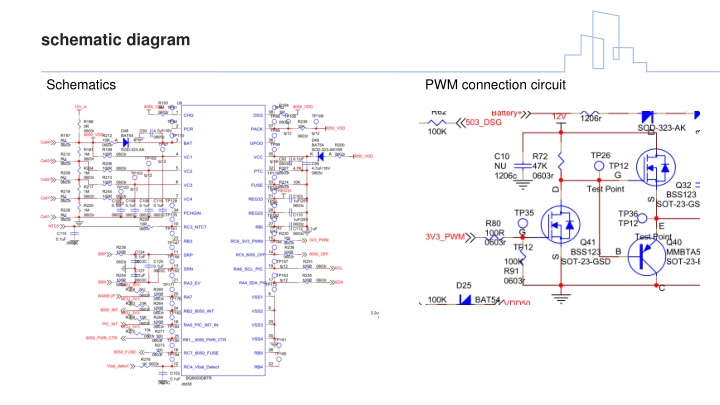
Diagnosis procedure(including swap test) on the output PWM abnormal PCBA 1.In the PC6 output PWM abnormal PCBA,We test to check if the cause of the PCBA abnormal is the BQ8050 chip itself a) Change the RC6 pin output PWM abnormal BQ8050 to the good PCBA for testing, and the good PCBA PWM function is abnormal. b) Change the RC6 pin output PWM normal BQ8050 to the bad PCBA for testing, and the bad PCBA PWM function is normal. c) Change the RC6 pin output PWM abnormal BQ8050 to the other bad PCBA for testing, and the bad PCBA PWM function is abnormal. 2.In addition to the RC6 pin function is abnormal, the other pins function is normal,such as communication, sampling Conclusion:The cause of the PCBA abnormal is the BQ8050 chip itself
Other simulation tests on the output PWM normal PCBA We also did other simulated damage tests on the output PWM normal PCBA ,try to reproduced this phenomenon 1.Test ESD :From contact 6K, air 8K, gradually increase to 24K, 2.Short-circuit :Pin RC6 with PWM output is short-circuited to B- 1 hour 3.External high positive voltage:Apply a positive voltage of 10V to RC6 externally for 30 minutes 4.External high negative voltage:Apply a negative voltage of 5V to RC6 externally for 10 minutes However, the PWM abnormal can t be reproduced


 on the output PWM")