Innovative Silicon Tracker Development for Tracking Applications
"Developed by a collaborative team of researchers, the APiX project aims to create an innovative Silicon tracker with avalanche pixel sensors for improved tracking applications. The project focuses on reducing Dark Count Rate effects and enhancing radiation hardness while optimizing sensor design and readout architecture."

Download Presentation

Please find below an Image/Link to download the presentation.
The content on the website is provided AS IS for your information and personal use only. It may not be sold, licensed, or shared on other websites without obtaining consent from the author. If you encounter any issues during the download, it is possible that the publisher has removed the file from their server.
You are allowed to download the files provided on this website for personal or commercial use, subject to the condition that they are used lawfully. All files are the property of their respective owners.
The content on the website is provided AS IS for your information and personal use only. It may not be sold, licensed, or shared on other websites without obtaining consent from the author.
E N D
Presentation Transcript
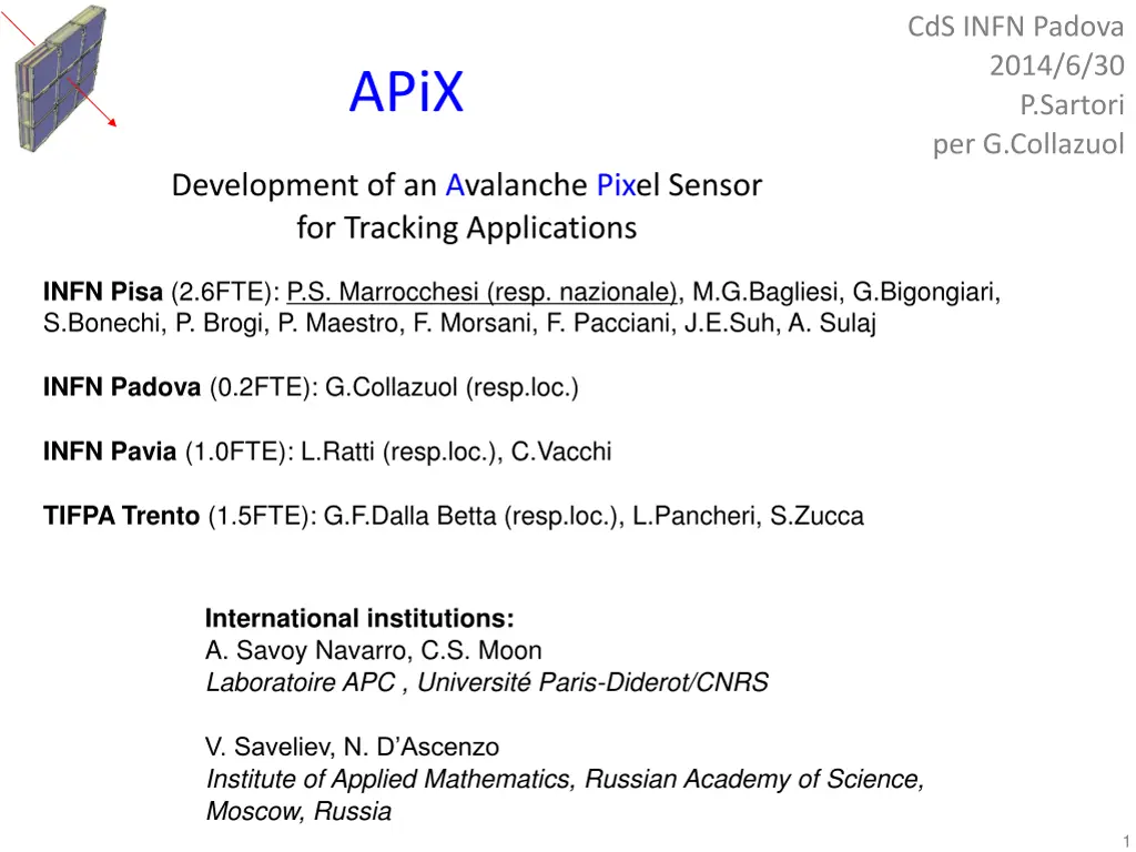
CdS INFN Padova 2014/6/30 APiX P.Sartori per G.Collazuol Development of an Avalanche Pixel Sensor for Tracking Applications INFN Pisa (2.6FTE): P.S. Marrocchesi (resp. nazionale), M.G.Bagliesi, G.Bigongiari, S.Bonechi, P. Brogi, P. Maestro, F. Morsani, F. Pacciani, J.E.Suh, A. Sulaj INFN Padova (0.2FTE): G.Collazuol (resp.loc.) INFN Pavia (1.0FTE): L.Ratti (resp.loc.), C.Vacchi TIFPA Trento (1.5FTE): G.F.Dalla Betta (resp.loc.), L.Pancheri, S.Zucca International institutions: A. Savoy Navarro, C.S. Moon Laboratoire APC , Universit Paris-Diderot/CNRS V. Saveliev, N. D Ascenzo Institute of Applied Mathematics, Russian Academy of Science, Moscow, Russia 1
Motivation Innovative Silicon tracker based on 1) thin sensitive volumes (pixels) 2) producing large signals 3) high timing resolution reduced material budget reduced power consumption enhanced S/N with simple electronics better radiation hardness high rate capability 2 G.Collazuol APIX 20140630
Overview The APiX concept CMOS avalanche cells providing internal gain for charged particle detection Coincidence between vertically aligned cells pairs to drastically reduce Dark Count Rate (DCR): dual tier Avalanche PiXel detector Main technological challenges: 1) CMOS sensor design: optimized for charged particle detection starting from the experience with CMOS SPAD development 2) Vertical integration of electronics for signal processing Mature technology: 3) Thinning 4) Readout architecture Workplan and milestones 3 G.Collazuol APIX 20140630
Basic detector element The basic element of the APiX detectoris an avalanche diode based on a CMOS process and operated in quenched Geiger mode - Several possible implementations in standard CMOS or CMOS imaging (CIS) or CMOS HV technologies - Inheritance from CMOS SPAD detector design Example: p+/n active area junction + Guard Ring + buried isolation layer Large internal gain provided by the detector itself no pre-amplification less power no amplitude measurement, pure binary information (hit/no hit) sensitive layer of the device is very thin, limited to the depleted region around the pn junction virtually no charge loss if the substrate is thinned down. readout electronics integrated in the same substrate as the sensor BUT - an avalanche detector is affected by a large dark count rate DCR ~ O(100 kHz/mm2) APiX concept: the coincidence of vertically aligned cells drastically reduces DCR problem 4 G.Collazuol APIX 20140630
APiX concept: dual tier Avalanche pixel detector Goal: reducing Dark Rate effects by using coincidence between two overlapping pixels (sensor pairs) Assuming a dark count rate DCR = 100 kHz/mm2 and t = 10ns coincidence, with N=50 m x 50 m pixels, the rate of fake 2 fold coincidence is 2 R2 t/N = 0.5 Hz/mm2 For 1cm2 detector is would be close to 50 Hz Main assets: Internal Gain reduces dramatically the material budget (few m sensitive thickness) Readout electronics on chip digital signal out reduction of the power consumption Vertical alignment and coincidence overcome the dark rate probability and sensitivity to photons Flexibility in layout improving detection efficiency for ionizing particles Accidental coincidence rate (estimate) Sensor Power consumption (readout power excluded) Assuming a 100MHz/cm2 hit rate on 1cm2 detector, the average current ~16 A @gain = 106 i.e. a power dissipation of about 0.32 mW/cm2 for 2 layers in the case of 10 V bias in the cell for full avalanche operation 5 G.Collazuol APIX 20140630
1) Main technological challenges: Implementation goals in CMOS for APiX are similar to the ones for CMOS SPAD (photon sensor): CMOS implementation 1) minimize the Dark Count Rate (DCR) in deep submicron technologies band to band tunneling typically increases due to the heavy doping concentration in the well implants increases DCR Shallow Trench Isolation (STI) oxide defects in Si interface DCR generation centers care must be taken in designing the Guard Ring structures 2) maximize detector efficiency For photon detection (as in the case of CMOS SPAD, SiPM) this means to maximize the Photon Detection Efficiency (PDE). However, in the case of particle detection (as proposed by APiX) photo absorbent structures limiting the Fill Factor (FF) are a minor issue. The layout can afford opaque structures (e.g. quenching resistor, poly lines, etc.) that are practically transparent to ionizing radiation Example of implementation of CMOS SPAD in 150nm CMOS process available at LFoundry: circular and square 10 m SPAD L. Pancheri, D. Stoppa, Low noise single Photon Avalanche Diodes in 0.15 m CMOS technology , IEEE Proc. of ESSDERC11 pp. 179 182 (2011) Technologies by LFoundry and XFAB will be exploited 6 G.Collazuol APIX 20140630
2) Main technological challenges: Vertical integration Vertical integration seems a natural choice for fabrication of a dual tier avalanche pixel sensor Virtually monolithic integration with chip to chip, chip-to-wafer, wafer-to-wafer vertical interconnection Various interconnection techniques available: micro bump bonding, direct bond interconnect, thermo compression Technologies by Tezzaron Semiconductor and Tohoku MicroTec (T-Micro) will be exploited 7 G.Collazuol APIX 20140630
3) Mature technologies: Sensor thinning Improves momentum resolution by reducing multiple scattering in multilayer silicon sensors Different approaches are available to thin wafer down even to 1 m based on oxide or p++ layers acting as etch stoppers Aptek Industries offers thinning services down to 25 30 m (10 15 m with 30% yield) at quite low prices ($ 30 per die, $ 287 minimum) 8 G.Collazuol APIX 20140630
4) Mature technologies: Readout electronics Very simple front end: TOP LAYER: converting the detector signal to a CMOS logic level BOTTOM LAYER: coincidence logic and r/o interface 9 G.Collazuol APIX 20140630
Applications The main goal of the project is the development of a detector for tracking (vertexing) applications, with low-material budget and low-power consumption; Use of CMOS technology ensures that high performance digital readout circuits can be monolithically integrated with the sensitive part of the device The outcome of this R&D activity can be beneficial to a number of other fields, including: research instrumentation; biomedical applications (e.g.: with beta-emitters); electron microscopy; CMOS imagers; other (industrial quality controls, homeland security, ...) 10 G.Collazuol APIX 20140630
Workplan and Milestones Milestone development of - basic sensor and - test structures of vertically aligned cell pairs First year simulation and design of avalanche pixel sensors (different pixel options for performance optimization) modeling of the vertical interconnected structure prototype fabrication and test vertical integration design of a multipurpose lab test bench Milestone fabrication and test of the APiX digital sensor Second year development of a small, vertically integrated detector prototype with integrated readout electronics test on a particle beam study of radiation tolerance of the device (from the standpoint of both ionization and bulk damage) Third year development of an APiX chip building block with relatively large active area test on a particle beam Milestone fabrication and test of the APiX building block Note: Delayed approval procedure for APIX in INFN time zero ~ spring 2014 11 G.Collazuol APIX 20140630
APIX Padova PC links Readout and Control Interface Board FPGA APIX Padova will take care of Readout and Control Board: - ReadOut and digital processing by FPGA - Control by controller/FPGA needed for instance to set SPAD enable mask (each SPAD can be enabled/disabled in case it generates too much DCR) or trigger configuration APIX Padova will contribute also with simulation of detector physics Nota: Tesi triennale Tommaso Boschi (relatore G.C.) Studi per lo sviluppo di tracciatori di particelle basati su pixel di silicio in regime Geiger effetti di particelle ionizzanti in Silicon PM 12 G.Collazuol APIX 20140630
APIX Padova Richieste 2015 Personale: G.Collazuol al 20% resp. loc. APIZ2_DTZ Richieste budget 2015: Missioni estere test beam CERN Consumo scheda elettronica readout per test primi chip 1.5k 5.0k Richieste servizi locali: Elettronica: 3 m.u. per disegno e realizzazione scheda Progettazione Meccanica: m.u. per struttura test beam Officina Meccanica: m.u. per struttura test beam 13 G.Collazuol APIX 20140630


 Main technological challenges:")
 Main technological challenges:")
 Mature technologies:")
 Mature technologies:")