Introduction to Digital Components in Computer Architecture
Delve into the realm of digital components in computer architecture, exploring binary-to-Gray and Gray-to-binary code converters, multiplexers, and demultiplexers. Understand the fundamental processes and logical expressions behind these crucial components.

Download Presentation

Please find below an Image/Link to download the presentation.
The content on the website is provided AS IS for your information and personal use only. It may not be sold, licensed, or shared on other websites without obtaining consent from the author.If you encounter any issues during the download, it is possible that the publisher has removed the file from their server.
You are allowed to download the files provided on this website for personal or commercial use, subject to the condition that they are used lawfully. All files are the property of their respective owners.
The content on the website is provided AS IS for your information and personal use only. It may not be sold, licensed, or shared on other websites without obtaining consent from the author.
E N D
Presentation Transcript
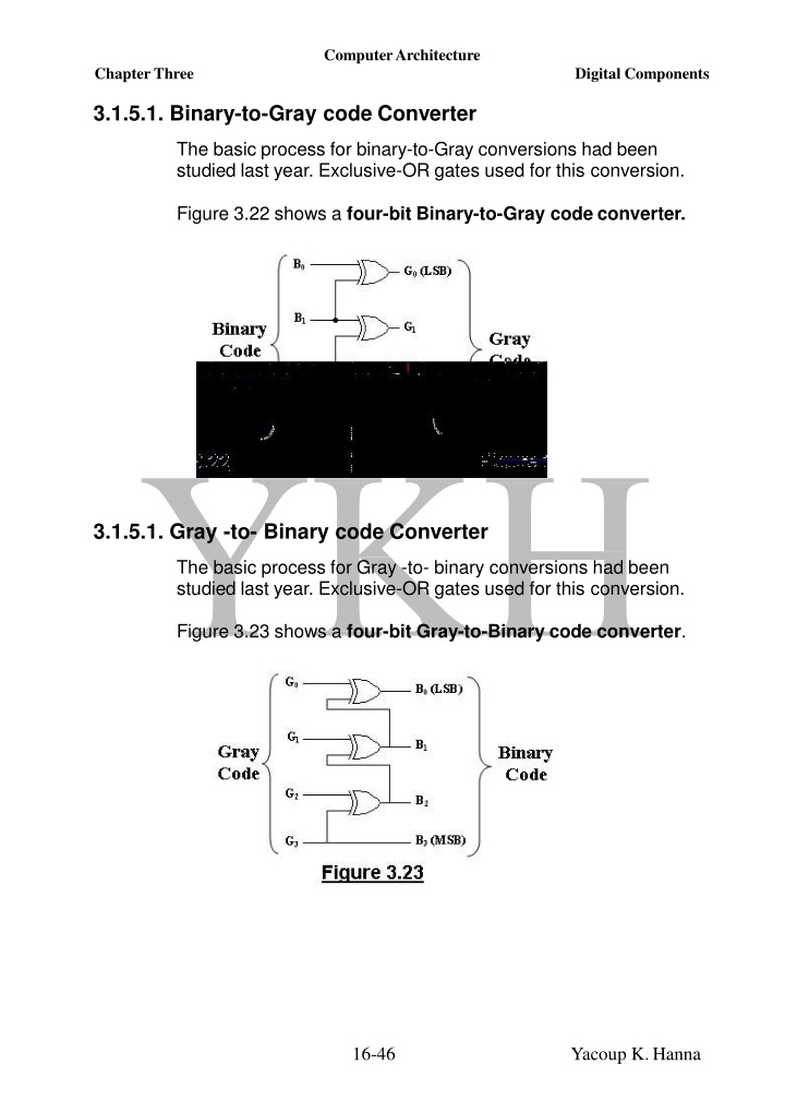
ComputerArchitecture ChapterThree Digital Components 3.1.5.1. Binary-to-Gray code Converter The basic process for binary-to-Gray conversions had been studied last year. Exclusive-OR gates used for this conversion. Figure 3.22 shows a four-bit Binary-to-Gray code converter. 3.1.5.1. Gray -to- Binary code Converter The basic process for Gray -to- binary conversions had been studied last year. Exclusive-OR gates used for this conversion. Figure 3.23 shows a four-bit Gray-to-Binary code converter. 16-46 Yacoup K.Hanna
ComputerArchitecture ChapterThree Digital Components 3.1.6. Multiplexers Multiplexer is a combinational circuit that selects binary information from one of 2ninput data lines and detects it to a single output line. A set of selection inputs select a particular input data line for the output. Multiplexer is called a Data selector, since it selects one of many data inputs and steers the binary information to the output. A 2n-to-1 Multiplexer has 2n input data lines, one output and n input selection lines whose combination determine which input data are selected for the output. A logic symbol for a 4-to-1-line Multiplexer is shown in figure 3.24. In reference to figure 3.24, the two data select inputs allow the data on the selected data input to pass through to the data output. A more suitable way to describe the operation of multiplexers is by means of a function table. The function table for the multiplexer is shown in table 3.9. The table illustrates the relationship between the four data inputs and the single output as a function of the selection inputs S1 & S0. For example, when the selection inputs are equal to 00, the output Y is equal to input I0, when the selection inputs S1S0 are equal to 01, the output Y is equal to I1and soon. Table 3.9 To design a combinational circuit that performs the multiplexing operation, first we derive the logical expression for the output in terms of the data input and the select inputs. This can be achieved as follows: - 17-46 Yacoup K.Hanna
ComputerArchitecture ChapterThree Digital Components 1.The data Y is equal to the data input I0 if and only if (S1=0 & S0=0) 2.The data Y is equal to the data input I1 if and only if (S1=0 & S0=1) 3.The data Y is equal to the data input I2 if and only if (S1=1 & S0=0) 4.The data Y is equal to the data input I3 if and only if (S1=1 & S0=1) 5. The total logical expression for the output Y therefore is as follows: 6. Figure 3.25 shows the logical diagram used to implement the above logic equation. Homework Construct multiplexers and one 2-to-1-line multiplexer. Use block diagrams for the three multiplexers. an 8-to-1-line multiplexer with two 4-to-1-line 18-46 Yacoup K.Hanna
ComputerArchitecture ChapterThree Digital Components 3.1.7. Demultiplexer A Demultiplexer is a device that takes data input from one line and distributes them to a given number of output lines. For this reason, Demultiplexer is known as a Data Distributor. A Demultiplexer reverses the multiplexing function. A more suitable way to describe the operation of Demultiplexer is by means of a function table as shown in table 3.10. The table illustrates the relationship between the single data input and the four outputs as a function of the selection inputs S1 & S0. Figure 3.26 shows a 1-line-to-4-line Demultiplexer logical diagram. From the logical diagram, it is clear that the two data select lines enable only one gate at a time, and the data appearing on the data input line would pass through the selected gate to the associated data output line. 19-46 Yacoup K.Hanna
ComputerArchitecture ChapterThree Digital Components 2. STOGAGE ELEMENTS All the digital circuits considered in chapters 2, and 3 were pure combinational digital circuits, where the outputs at any given time are entirely dependent on the inputs that are present at any time. Practically most of digital system consists of storage element in addition to a combinational circuit to form what is called a Sequential circuit. The synchronous sequential circuit is the most common type of sequential circuit encountered in practice. Synchronous sequential circuits employ signals that affect the storage elements only at discrete instants of time. Synchronization means that the output of the storage element changes state only at a specified point on a triggering input called the Clock; that is, changes in the output occur in synchronization with the clock. The device that produces a periodic train of clock pulses called a Clock Pulse Generator. 1. Flip-Flops The storage elements employed in clocked sequential circuits called Flip-Flops. A Flip-Flop is a binary cell capable of storing one bit of information (0 or 1). A flip-flop has two outputs, one for the normal value and the other for the complemented value. This storage element maintains a binary state until directed by a clock pulse to switch states. Different types of flip-flops presented, the differences among various types are in the number of inputs they possess and in the manner in which the inputs affect the binary state. SR Flip-Flop Figure 3.28 shows the symbol of SR Flip-Flop. Figure 3.28 SR flip-flop has three inputs and two outputs. The three inputs are: 1. S stands for the SET 2. R stands for the RESET 3. C stands for the CLOCK. The arrowhead-shaped symbol in front of the letter C designates a dynamic input. The dynamic 20-46 Yacoup K.Hanna
ComputerArchitecture ChapterThree Digital Components indicator symbol denotes the fact that the flip-flop responds to a positive transition (from 0 to 1) of the input clock signal. The two outputs are: 1. Q Stands for the normal output state 2. Q Stands for the complemented output state, a small circle used to indicate this output. The operation of the RS flip-flop can be summarized as follows: 1. For no signal at the clock input, the output of the flip-flop is unchanged irrespective of the values at inputs S and R. 2. When the clock signal changes from 0 to 1, the output affected according to the inputs S and R as follows: a. For S = 1 and R = 0, the output Q is set to1. b. For S = 0 and R = 1, the output Q is cleared to 0. c. For S = 0 and R = 0, the output Q does not change, i.e. 1) (t). d. For S =1 and R = 1, the output is unpredicted, i.e. the output may go to 0 or 1. ( According to above, the characteristic table of the RS flip-flop is shown in table 3.11. Table 3.11 Notes 1. Q ( t ) is the binary state of the Q output at a given time called Present State. 2. Q ( t+1 ) is the binary state of the Q output after the occurrence of a clock transition called NextState. 3. The SR flip-flop should not be pulsed when S=R=1 since it produces an indeterminate next state, and hence this is the reason the SR flip-flop rarely used in practice. D Flip-Flop 21-46 Yacoup K.Hanna
ComputerArchitecture ChapterThree Digital Components The D (data) flip-flop is a modification of SR flip-flop where, an SR Flip-Flop is converted to a D flip-flop simply by inserting an inverter between S and R and assigning the symbol D to the resultant single input. Figure 3.29 shows the symbol of D Flip-Flop. Figure 3.29 D flip-flop has two inputs and two outputs. The two inputs are: 1. D stands for the single data input. 2. C stands for the CLOCK. The two outputs are: 1. Q Stands for the normal output state 2. Q Stands for the complemented output state. The operation of the D flip-flop can be summarized as follows: 1. For no signal at the clock input, the output of the flip-flop is unchanged irrespective of the D value. 2. When the clock signal changes from 0 to 1, the output affected according to the input D as follows: a. For D = 1 , the output Q is set to 1. b. For D = 0 , the output Q is cleared to 0. According to above, the characteristic table of the D flip-flop is shown in table 3.12. Table 3.12 Notes 1. The relationship between the next state Q (t+1) and the D input can be expressed by a characteristic equation: Q(t+1) = D (3.1) 2. The disadvantage of the D flip-flop is that its characteristic table does not have a no change condition Q (t+1) = Q (t). JK Flip-Flop 22-46 Yacoup K.Hanna
ComputerArchitecture ChapterThree Digital Components A JK flip-flop is the refinement of the SR flip-flop in which the indeterminate condition of the SR flip-flop (i.e. the state of the input when S=R=1) is defined in the JK flip-flop. Figure 3.30 shows the symbol of JK Flip-Flop. Figure 3.30 JK flip-flop has three inputs and two outputs. The three inputs are: 1. J stands for the SET 2. K stands for the RESET 3. C stands for the CLOCK. The two outputs are: 1. Q Stands for the normal output state 2. Q Stands for the complemented output state. The operation of the JK flip-flop can be summarized as follows: 1. For no signal at the clock input, the output of the flip-flop is unchanged irrespective of the values at inputs J and K. 2. When the clock signal changes from 0 to 1, the output affected according to the inputs J and K as follows: a. For J = 1 and K = 0, the output Q is set to 1. b. For J = 0 and k = 1, the output Q is cleared to 0. c. For J = 0 and K = 0, the output Q does not change, i.e. Q(t = 1) = Q(t) . d. For J =1 and K = 1, the output is complemented, i.e. ???? . According to above, the characteristic table of the JK flip-flop is shown in table 3.13. Table 3.13 T Flip-Flop 23-46 Yacoup K.Hanna
ComputerArchitecture ChapterThree Digital Components The (Toggle) T Flip-Flop is obtained from a JK Flip-Flop when the inputs J and K are connected together to provide a single input designated by T. Figure 3.31 shows the symbol of T Flip-Flop. Figure 3.31 T flip-flop has two inputs and two outputs. The two inputs are: 1. T stands for the single data input. 2. C stands for the CLOCK. The two outputs are: 1. Q Stands for the normal output state 2. Q Stands for the complemented output state. The operation of the T flip-flop can be summarized as follows: 1. For no signal at the clock input, the output of the flip-flop is unchanged irrespective of the T value. 2. When the clock signal changes from 0 to 1, the output affected according to the input T as follows: a. For T = 0 , the output Q is unchanged, i.e. b. For T = 1 , the output Q is complemented, i.e. . . According to above, the characteristic table of the T flip-flop is shown in table 3.14. Table 3.14 3.2.2. Flip-Flop s Excitation Tables 24-46 Yacoup K.Hanna
ComputerArchitecture ChapterThree Digital Components In the previous article, the characteristic tables of different type of Flip- Flop s have been discussed by which one can specify the next state of the flip-flop when the inputs and the present state are known. For a design purposes, what is called a Flip-Flop excitation tables is required since we know the required transition from the present state to the next state and we wish to find the flip-flop input conditions that will cause the desired transition. Usually the excitation table consists of two columns, Q (t) and Q (t+1), and a column for each input to show how the required transition is achieved. There are four possible transitions from present state Q (t) to the next state Q (t+1). The required input conditions for each of the four transitions for a given flip-flop can be derived from the information characteristic table. given in the corresponding The symbol x in the following excitation tables represents a don't- care condition; i.e. it does not matter whether the input to the flip- flop is 0 or 1. SR Flip-Flop Excitation Table Table 3.15 shows the excitation table of SR flip-flop. Table 3.15 D Flip-Flop Excitation Table 25-46 Yacoup K.Hanna
ComputerArchitecture ChapterThree Digital Components Table 3.16 shows the excitation table of D flip-flop. Table 3.16 1. JK Flip-Flop ExcitationTable Table 3.17 shows the excitation table of JK flip-flop. Table 3.17 2. T Flip-Flop ExcitationTable Table 3.18 shows the excitation table of the T flip-flop. Table 3.18 3.3. SEQUENTIAL CIRCUITS 26-46 Yacoup K.Hanna
ComputerArchitecture ChapterThree Digital Components A Sequential Circuit is defined as an interconnection of flip-flops and logic gates. Previously we assign to a interconnection of logic gates as a Combinational Circuit. When the combinational circuit included with flip-flops, the overall logical circuit is classified as a Sequential Logical Circuit. Figure 3.32 shows a general block diagram of a Sequential circuit. Figure 3.32 The diagram above shows the combinational circuit which receives binary signals from external inputs and the flip-flops output. The outputs of the combinational circuit go to external outputs and to flip- flops input. The combinational circuit determines the binary value to be stored in the flip-flops after each clock transition. The outputs of flip-flops, in turn, are applied to the combinational circuit inputs and determine the circuit behavior. The above process shows that the outputs of a sequential circuit are functions of both external inputs and the present state of the flip- flops. The next state of the flip-flops is a function of their present states and the external inputs. As a summarization, a Sequential circuit is specified by a time sequence of external inputs, external outputs, and internal flip-flops binary states. 3.3.1. Sequential Circuit Design 27-46 Yacoup K.Hanna
ComputerArchitecture ChapterThree Digital Components The design procedure of a Sequential Circuit consists of the following steps:- 1. State the Circuit Specifications. 2. Translating the circuit specifications into a StateDiagram. 3. Obtaining the Excitation Table from the State Diagram. 4. Obtaining the Sequential Circuit Diagram from the Excitation Table. The above procedure for designing a sequential circuit will be demonstrated by the following example: - 1. Circuit Specifications. Design a sequential circuit called a 2-bit binary counter that goes through a sequence of repeated binary states 00, 01, 10, and 11 for the input y = 1, and the state of the circuit remains unchanged for the input y = 0. Note that the input y is called the Control Variable that specifies when the count should proceed. 2. State Diagram. The state diagram of the above sequential circuit is shown in figure 3.33. Figure 3.33 From the state diagram above, it is clear that when y = 0, the state of the circuit remains unchanged. When y = 1, the circuit follow the binary count as long as y = 1. Note that the state follows 11 is 00. The state of the flip-flops is considered as the outputs of the counter. Two flip-flops A and B are needed to represent the two bits representing each of the four states. 3. Excitation Table. 28-46 Yacoup K.Hanna
ComputerArchitecture ChapterThree Digital Components The excitation table in general consists from the following: - a. Number of columns to represent the present state. b. Number of columns to represent the next state. c. Number of columns to represent the inputs. d. Number of columns to represent the flip-flops inputs. The flip- flop input conditions are a function of the type of flip-flop used. Note. The columns mentioned in a, b, and c above constitutes what is called State Table. Now retaining back to our example and using the excitation table of a JK flip-flop specified in table 3.17, the overall Excitation Table of the sequential circuit is shown in table 3.19 below. Table 3.19 Output State Transitions Present State A B 0 0 0 1 1 0 1 1 0 0 0 1 1 0 1 1 Flip-Flops Inputs Next State A 0 0 1 1 0 1 1 0 Input Y JA KA JB KB B 0 1 0 1 1 0 1 0 0 0 0 0 1 1 1 1 0 0 x x 0 1 x x x x 0 0 x x 0 1 0 x 0 x 1 x 1 x x 0 x 0 x 1 x 1 As we indicated before, two JK flip-flops are used to represents the two states in the required counter. We denote the inputs of flip-flop A by JAand KA, and those of flip-flop B by JBand KB. To illustrate how the excitation table is implemented, we proceed as follows: - a. The three columns (Present State, Input, and Next State) under Output State Transitions main column are deduced from the state of the circuit specification given for the required sequential circuit (i.e. 2-bits binary counter). For example, in the first row of table 3.19, we have the present state 00 with input 0, the next state must be 00 (unchanged). 29-46 Yacoup K.Hanna
ComputerArchitecture ChapterThree Digital Components The same appeared in the second, third, and fourth rows (i.e. no state change) since the input y = 0. For the remaining four last rows, with the input x = 1, the next state changes to the following state of the present state. b. The two columns (JA KA and JB KB) under Flip-Flop Inputs main column are deduced from, the Present State and Next State given in the same row according and by using the excitation table of JK flip-flop given in table 3.17 rewritten below. For example, in the first row of table 3.19, we have a transition for flip-flop A from 0 in the present state Q (t) = 0 to 0 in the next state Q (t+1) = 0 in a JK flip-flop requires that input J = 0 and input K = x. So 0 and x are copied in the first row under JA and KA, respectively. Since the first row also shows a transition for flip-flop B from 0 in the present state to 0 in the next state, 0 and x are copied in the first row under JBand KB respectively. A second example, the second row of table 3.19, we have a transition for the flip-flop A from 0 in the present state to 0 in the next state (i.e. the same as in the first row); therefore, 0 and x are copied in the first row under JA and KA, respectively. Since the second row also shows a transition for flip-flop B from 1 in the present state to 1 in the next state, x and 1 are copied in the second row under JBand KB respectively. A third example, in the sixth row of table 3.19, we have a transition for flip-flop A from 0 in the present state Q (t) = 0 to 1 in the next state Q (t+1) = 1 in a JK flip-flop requires that input J = 1 and input K = x. So 1 and x are copied in the sixth row under JAand KA, respectively. Since the sixth row also shows a transition for flip-flop B from 1 in the present state to 0 in the next state, x and 1 are copied in the first row under JB and KB respectively 30-46 Yacoup K.Hanna


![❤Book⚡[PDF]✔ The Apollo Guidance Computer: Architecture and Operation (Springer](/thumb/21611/book-pdf-the-apollo-guidance-computer-architecture-and-operation-springer.jpg)