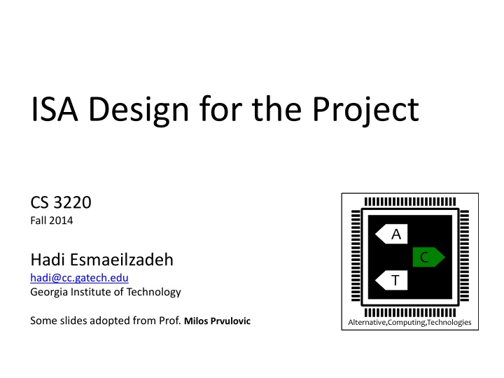
ISA Design for Project CS 3220 Fall 2014 with A.C. Hadi Esmaeilzadeh
ISA decisions involving players, HW/SW co-design, CISC vs. RISC, memory access, ALU instructions, and branches. Emphasizing simplicity, coding ease, and processor design considerations.

Download Presentation

Please find below an Image/Link to download the presentation.
The content on the website is provided AS IS for your information and personal use only. It may not be sold, licensed, or shared on other websites without obtaining consent from the author.If you encounter any issues during the download, it is possible that the publisher has removed the file from their server.
You are allowed to download the files provided on this website for personal or commercial use, subject to the condition that they are used lawfully. All files are the property of their respective owners.
The content on the website is provided AS IS for your information and personal use only. It may not be sold, licensed, or shared on other websites without obtaining consent from the author.
E N D
Presentation Transcript
ISA Design for the Project CS 3220 Fall 2014 A C Hadi Esmaeilzadeh hadi@cc.gatech.edu Georgia Institute of Technology T Some slides adopted from Prof. Milos Prvulovic Alternative,Computing,Technologies
Project ISA Who are the players? Are we doing HW/SW co-design? We will be designing processor, need an ISA What do we want in our ISA Easy to decode (you ll have to write this in Verilog) Easy to write assembler for (you ll have to write one) Easy to write applications for (you ll do this, too) Similar tradeoff involved in designing real CPUs Plus backward compatibility But for CS 3220 we don t want backward compatibility! Encourages laziness and cheating (Verilog code may already be posted somewhere) 2
ISA decisions CISC or RISC? Definitely RISC (much easier to design) Fixed-size or variable size? Definitely fixed (fetch and decode much easier) How many things can be read or written Each register read (>1) complicates register file Each register write (>1) complicates register file a lot! Each memory read or write (>1) creates lots of problems (memory ports, pipeline stages, hazards). 3
Which instructions? Memory! How will we access memory Do we use only LD/ST, or do we allow memory operands in other kinds of instructions? Only LD/ST is far simpler to implement because: Mem operands in ADD, SUB, etc. require many flavors for each instruction (tough to decode) And we need to describe the entire decoding logic in Verilog Don t want multiple memory accesses per inst! Even one memory stage in the pipeline is complex enough OK, we ll have LW, SW 4
Which instructions? ALU! Let s have some arithmetic ADD, SUB, what else? How about some logic? Option 1: AND, OR, NOT, XOR, etc. Option 2: Let s just have one! Which one? NAND! Can fake others using NAND, e.g. NOT A is A NAND A Let s use Option 1 but not go overboard Easier to write assembler, easier to decode But leave room (unused opcodes) for more Comparisons? It depends Option 1: Conditional branches do comparisons Option 2: Comparison instructions, one cond. branch Option 3: Mix of the two 5
Speaking of branches Conditional branches PC relative, need decent-sized offset operand Hard to write if-then-else and loops if branch only goes e.g. 3 instructions forward or back How will we call procedures? Option 1: Special branch that saves return address Option 2: Save RA in SW, use normal branch How will we return from procedures? Option 1: Specialized RET Option 2: Jump-to-address-in-register (JR) Let s have only one call/jump/return inst for now! Similar to JALR instruction from CS 2200 Syntax would be JAL Rdst,Imm(Rsrc) 6
Conditional branches? Typical conditional branches BEQ R1,R2,Label ; Go to Label if R1==R2 Can also have BLT, BLE, BNE, BGT, BGE Need to encode two registers in the instruction BEQZ R1, Label ; Go to Label if R1==0 Can also have BNEZ, BLEZ, etc. Need to encode only one register in the instruction (so we can have a 6-bit offset) Could have implicit operand, e.g. always R1 BEQZ Label ; If R1==0 go to Label Bad: R1 won t be very useful for anything else 7
How many registers? Need at least 2 to do ALU operations Plus one to be a stack pointer Plus one to save return address Unless we want to save it directly to memory Nice to have a few extra One for return value (to avoid saving it to stack) Some to pass parameters? Need at least 2 (more is even better) Need at least one for system use We ll work on this in the last two projects OK, this is already 8 or more, so let s have 16 When writing code in assembler, we ll see that more is better 8
Size of instruction word? Bits in instruction word? Hmm, let s see Need room for opcode How many types of instructions do we have? Can have a secondary opcode for some (e.g. for ADD,SUB, etc.) Need room for register operands Do we want 1, 2, or 3 or those? 3! This will use 12 bits in the instruction word Need room for immediate operands The more the better, but too few will be a problem Let s have 32-bit instruction word 8 not really an option (not enough room) 16 is very tight (with 16 regs, only 4 bits left for opcode) So let s do 32 (allows large offsets, more opcodes, etc.) 9
Register size? How about 8? Will need multi-word values often (e.g. loop counters) PC must be larger than this, procedure calls get tricky Can we do with 16? Most loops and programs will be OK Immediate operand can load entire constant (nice) Can display entire word on HEX display But it makes sense to have 32-bit registers Same as instruction word Almost never have to worry about overflows and such 10
Memory addressing? Byte-addressed or word-addressed? Word-addressed is simpler Only need LD/ST instruction, vs. LW/SW, LB/SB, etc. Don t have to worry about alignment But Hard to switch apps to byte-addressed later Can t use e.g. 16-bit memory locations We can achieve most of the HW simplicity if we require word-alignment So we ll have byte-addressed aligned LW/SW only Can drop alignment limitations later if we want to But can add LB/SB, LH/SH later if we want to 11
ISA definition How many bits for the opcode? For insts w/ 3 reg operands, 12 bits already used Great, leaves 20 bits for opcode! But For insts w/ 2 reg and 1 imm operand E.g. LW R1,-4(R2), ADDI R1,R2,64, BNE R1,R2,Label Imm and opcode must fit in 24 bits (10 used for regno) Let s have a 16-bit immediate and 4-bit opcode Will make register number decoding a bit easier Few reach issues in branches and LW/SW Fairly large constants in ADDI, SUBI, ANDI, etc. We have 16 opcodes Won t be enough LW, SW, Will needa a trick called secondary opcode to for >16 instructions 12
Instruction Format Thus Far wire [3:0] op1; // Primary opcode wire [3:0] rd,rs,rt; // Register operands wire [15:0] imm; // 16-bit immediate operand assign {op1,rd,rs,rt,imm}=iword; Decoding of register numbers is trivial But only 16 different instructions? LW, SW (and leave room for LH, SH, LB, SB) ADDI, ADD, SUB, AND, OR, XOR, NOT BEQZ, BNEZ, JAL This is already 16 What if we want to add more later, e.g. MUL? 13
Primary/Secondary Opcode Have a smaller primary opcode (our four bits) Instructions without an imm operand have 16 free bits ADD Rd,Rs,Rt uses 16 bits for primary opcode and regs Instructions with an imm but only two regs have 4 free bits LW Rd,Imm(Rs) does not use the Rt field Also ADDI Rd,Rs,Imm, SUBI, etc. SW Rt,Imm(Rs) does not use the Rd field Also BEQ Rs,Rt,Imm, etc. Idea: Use these extra bits for a secondary opcode Uses only one primary opcode for a family of ALU instructions Secondary opcode => the actual operation Primary opcode of 0000 now means 3-reg ALU inst Imm field unused => Secondary opcode can be up to 16 bits We ll use only 6 for now (enough for many insts) E.g. 000000 is NOP, 000001 is ADD, etc. Primary opcode of 1000 now means 2-reg load inst Secondary opcode in Rt field (4 bits), e.g. 0000 is LW 14
Assign Primary Opcodes Does it matter which insts get which opcode? E.g. ALU Rd,Rs,Rt 0000, ALU Rd,Rs,Imm is 0001, etc.? Make the decoding easy! After we read the primary opcode, need to look at secondary opcode to finish decoding Let some opcode bits tell us where the op2 is! Assigning opcode numbers as a list is messy So we use an opcode chart 15
Opcode Chart We have 4-bit primary opcodes (2 x 2 bits) Less significant 2 bits 00 01 10 11 More significant 2 bits 00 ALUR CMPR 01 Store Bcond 10 ALUI Load CMPI 11 4 Feb 2014 Project ISA 16
Load (op1=1001) Opcode Chart We have a 4-bit secondary opcode instead of Rt Less significant 2 bits 00 01 10 11 More significant 2 bits Will add these later 00 LW LH LB 01 10 Why not here? No particular reason! 11 18
Store (op1=0101) Opcode Chart We have a 4-bit secondary opcode instead of Rd Less significant 2 bits 00 01 10 11 More significant 2 bits Will add these later 00 SW SH SB 01 10 Why not here? Symmetry w/ Load! 11 19
ALUR (op1=0000) Opcode Chart 16-bit secondary opcode instead of Imm We ll keep bits 11:4 at zero, use only [3:0]. Why? Less significant 2 bits 00 01 10 11 More significant 2 bits 00 ADD SUB 01 AND OR XOR 10 11 NAND NOR NXOR 20
ALUI (op1=1000) Opcode Chart 4-bit secondary opcode instead of Rt Where should ADDI, SUBI, etc. go in this table? Less significant 2 bits 00 00 01 01 10 10 11 11 More significant 2 bits 00 00 ADDI SUBI 01 01 ANDI ORI XORI 10 10 11 11 NANDI NORI NXORI 21
CMP/CMPI/Bcond Opcode Chart 4-bit secondary opcode instead of Rd All have the same op2 decoding Less significant 2 bits 00 00 01 01 10 10 11 11 False, True? Why 0000 for EQ? Why GTE and GT swapped here? More significant 2 bits 00 00 False EQ LT LTE 01 01 EQZ LTZ LTEZ 10 10 True NE GTE GT 11 11 NEZ GTEZ GTZ 22
Constant into register? How would you put a 32-bit constant into a reg? Start with zero in a register (easy, e.g. XOR R1,R1,R1) ADDI a 16-bit constant OK, half-way there! What now? Errr shift up 16 places! ADD R1,R1,R1 is R1<<1, just do this 16 times? We ll want to have proper shift instructions To load a large constant: XOR, ADDI, SLL, ADDI Let s add a MVHI instruction! The upper 16 bits come from the immediate operand What about the lower 16 bits? Zero them out! Can MVHI then ADDI to load a 32-bit constant 23
Adding MVHI to the ALUI op2 Chart Less significant 2 bits 00 00 01 01 10 10 11 11 More significant 2 bits 00 00 ADDI SUBI 01 01 ANDI ORI XORI 10 10 MVHI 11 11 NANDI NORI NXORI 24
JAL? JAL Rd,Imm(Rs) RD = PC + 4 Jump to RS + Imm Can t be in the Bcond op2 table! Does not do a comparison But this is similar to B (Bcond with True condition) Writes to Rd! Can t use Rd for op2! 25
JAL op1? Not using Rt => Can use op1=1011 Should we have op2 for JAL? Unlikely to have more JAL-like instructions BUT! Less significant 2 bits Don t waste opcodes! op1=1011 (op2 in Rt) op2=0000 00 01 10 11 More significant 2 bits 00 ALUR CMPR op2 = imm op2 = Rd 01 Store Bcond op2 = Rt 10 ALUI Load CMPI JAL 11 26
Instruction Format {op1,rd,rs,rt,12 b0,op2} This format is used when op1 is ALUR or CMPR ALUR: rd = rs OP2 rt CMPR: rd = (rs OP2 rt)?1:0 Instruction mnemonics are F (False), T (for True), EQ, NE, etc. {op1,op2,rs,rt,imm} This format is used when op1 is Store or Bcond Store: mem[rs + sxt(imm)]=rt Bcond: if(rs OP2 rt) PC=PC+4+(sxt(imm)*4) Instruction mnemonics are BF, BT, BEQ, BNE, etc. {op1,rd,rs,op2,imm} This format is used when op1 is ALUI, CMPI, Load, or JAL ALUI: rd = rs OP2 sxt(imm) CMPI: rd=(rs OP2 sxt(imm))?1:0 Instruction mnemonics are FI, TI, EQI, NEI, etc. Load: rd=mem[rs + sxt(imm)] JAL: rd<=PC+4; PC<=rs+4*sxt(imm); Note <= here! What should JAL R1,0(R1) do? 27
Assembler syntax Instruction opcodes and register names Are reserved words (can t be used as labels) Appear in either lowercase or uppercase If there is a destination register, it is listed first Labels Created using a name and then : at the start of a line Corresponds to the address where label created Immediate operands number or label If number, hex (C format, e.g. 0xffff) or decimal (can have - sign) If label, just use the name of the lable (without : ) For PC-relative, the immediate field is label_addr-PC-4 For other insts, the immediate field is 16 least-significant bits of label_addr 28
Register Names Each register has multiple names R0..R3 are also A0..A3 (function arguments, caller saved) R3 is also RV (return value, caller saved) R4..R5 are also T0..T1 (temporaries, caller saved) R6..R8 are also S0..S2 (calee-saved values) R9 reserved for assembler use R10..R11 reserved for system use (we ll see later for what) R12 is GP (global pointer) R13 is FP (frame pointer) R14 is SP (stack pointer) R15 is RA (return address) Stack grows down, SP points to lowest in-use address 29
Assembler syntax .ORG <number> Changes current address to <number> .WORD <value> Places 32-bit word <value> at the current address <value> can be a number or a label name If label name, value is the full 32-bit label_addr .NAME <name>=<value> Defines a name (label) with a given value (number) Otherwise we would have to name constants using .ORG 1 One: 30
Pseudo-instructions Do not actually exist in the ISA Translate into existing instructions Can use R9 (see below) That s why we reserved it for assembler use We will have (for now) NOT Ri,Rj => NAND Ri,Rj,Rj CALL Imm(Ri) => JAL RA,Imm(Ri) RET => JAL R9,0(RA) JMP Imm(Ri) => JAL R9,Imm(Ri) 31
Memory? Separate inst and data memory? Good: Our design will be faster, cheaper Bad: How does one load programs into memory? We ll have separate imem and dmem for now We ll see later how to unify them How much memory? There are 239,616 memory bits on-chip, so 8kB (2048 32-bit words) of imem 8kB (2048 32-bit words) of dmem Leaves about half of memory bits on the FPGA chip (for register file, debugging in SignalTap, etc.) 32
Input/Output? We want our programs to Read SW, KEY (so we can interact with it) Write to HEX, LEDG, LEDG Maybe some more I/O Need instructions for this! Special instruction for each device, e.g. WRLEDG Extensions are hard (change processor as each device added) Special IN/OUT instructions Assign addresses to devices, then use IN/OUT to read/write Memory-mapped I/O (this is what we ll use) Each device gets a memory address, LW/SW can be used for I/O Can t use those memory locations as normal memory! 33
Prelude to Assignment 2 Don t panic (yet)! Will do much of the design in lectures! Write an assembler Reads assembler listing for this project ISA Including pseudo instructions Outputs a file with 2048 32-bit words of memory in the .mif file format (Test2.mif, Sorter2.mif) Verilog design of a multi-cycle processor Implements this ISA, PC starts at (byte address) 0x40 Uses Sorter2.mif to pre-load its 8kB memory SW to address 0xF0000000 displays bits 15..0 as hexadecimal digits on HEX display SW to address 0xF0000004 displays bits 9..0 on LEDR SW to address 0xF0000008 displays bits 7..0 on LEDG LW from address 0xF0000010 reads KEY state Result of LW should be 0 when no KEY pressed, 0xF when all are pressed This means we actually need LW to get {28 b0,!KEY} LW from address 0xF0000014 reads SW state The 32-bit value we read should really be {22 b0,SWd) SWd is a debounced value of SW 34


 Opcode Chart")
 Opcode Chart")
 Opcode Chart")
 Opcode Chart")