JESD204B Interface and Timing Signals
Explore the evolution of JESD204 standard from its inception to the latest revisions, including JESD204B. Learn about the specifications, subclasses, and timing signals terminology associated with JESD204. Discover the significance of JESD in LVDS and CMOS systems and its impact on data converters and output buffers. TI Information NDA Required.

Download Presentation

Please find below an Image/Link to download the presentation.
The content on the website is provided AS IS for your information and personal use only. It may not be sold, licensed, or shared on other websites without obtaining consent from the author. If you encounter any issues during the download, it is possible that the publisher has removed the file from their server.
You are allowed to download the files provided on this website for personal or commercial use, subject to the condition that they are used lawfully. All files are the property of their respective owners.
The content on the website is provided AS IS for your information and personal use only. It may not be sold, licensed, or shared on other websites without obtaining consent from the author.
E N D
Presentation Transcript
JESD204B Overview e2e.ti.com (TI Support Forum) July 2014
www.ti.com, select data converters, then High Speed ADC, then JESD204B Interface
Outline JESD204 A & B History Timing Signals Transport Layer, Scrambler, Data Link Layer, Control Symbols, and Physical Layer Deterministic Latency Subclass 0, 1, 2 Configuration Parameters Error Reporting Timing Signals
Introduction: Why JESD? In LVDS and CMOS systems, package size, board area and power consumption dominated by output buffers rather than the data converter. DAC DAC TI Information NDA Required
JEDEC (Joint Electron Device Engineering Council) now called JEDEC Solid State Technology Association created JEDEC Standard JESD204 Serial Interface for Data Converters TI Information NDA Required
Original Spec JESD204 April 2006 Defines a single lane high speed serial link connected to single/multiple data converters with speed up to 3.125Gbps. TI Information NDA Required
REVISIONS JESD204A April 2008 Revision A extends the support to multiple aligned lanes with multipoint link. Maximum supported speed is the same, 3.15Gbps. TI Information NDA Required
JESD204B July 2011 Subclasses: 0 (backward compatible), 1, 2 Support for Deterministic Latency Frame clock changed to device clock Serial lanes speeds up to 12.5Gb/s TI Information NDA Required
JESD204 Timing Signals/Terminology Device Clock System clock from which the device s frame, sampling, LMFC clocks are derived (externally applied) SYSREF Timing phase reference from which LMFC clocks are generated in subclass 1 implementations (externally applied) Source synchronous with device clock Rising edge event sampled by device clock determines LMFC alignment Periodic, Gapped-periodic, One-shot types TI Information NDA Required
JESD204 Timing Signals/Terminology Frame Clock (Core CLK) The frame coming out of the transport layer is aligned to the frame clock. As per JESD204B standard, frame clock period in all the TX and RX devices must be identical. Sample Clock Sample clock is aligned to a sample boundary. If there is only one sample per converter in a single frame cycle, then sample clock is the same as frame clock. If there are multiple samples per converter per frame clock cycle, then sample clock is an integer multiple of the frame clock. Local Multiframe Clock (LMFC) K * Frame Clock LMFC is aligned to a multiframe boundary which in turn consists of K number of frames. In order to synchronize transmission on all lanes (single or multipoint link), LMFC of all the converter devices are aligned with the LMFC of logic device. All TX and RX devices in a system must have identical LMFC period. TI Information NDA Required
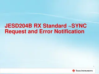
JESD204 Timing Signals/Terminology SYNC Receiver to Transmitter. Used for device synchronization and link error reporting Synchronization requests Subclass 2 implementations use SYNC as a phase reference for LMFC Options for distributing SYNC to multiple devices Standard defines SYNC~ (active low) signaling TI Information NDA Required
JESD204 Layers TI Information NDA Required
Example Functional Diagram for data transmission and reception between two devices on the link TX device (ADC or FPGA) Parallel to -serial mapping 8B/10B encoding and character insertion for lane alignment Device Clock Clock Source SYSREF Clock SYNC~ SYSREF Clock Device Clock 8B/10B decoding and character detection for lane alignment serial to -parallel mapping RX device (DAC or FPGA) 13
Transport Layer Overview Maps the data octets frames consisting of multiple octets Adds optional control bits to samples if needed Control bits can be used to communicate status information, mark an inactive converter on the link or control receiver operation Distinguishes the possible combinations of device/links/lanes/etc. Single converter connected to single lane link Single converter connected to multiple lanes link Multiple converters in a converter device connected to a single lane link Multiple converters in a converter device connected to multiple lanes link TI Information NDA Required
Transport Layer Overview TI Information NDA Required
Transport Layer Parameters Important parameters associated with transport layer include L M F S CS # of control bits per conversion sample # of lanes per converter device # of converters per device # of octets per frame (per lane) # of samples per converter per frame clock cycle TI Information NDA Required
Transport Layer Example Example: 11-bit octal ADC converter L = 4, M = 8, F = 4, S = 1, CS = 2 TI Information NDA Required
Scrambling Scrambling randomizes data and spreads the spectral content to reduce spectral peaks that could cause EMI and interference problems Transport layer output may be optionally scrambled with the polynomial: 1 + x14 + x15 The RX descrambler self-synchronizes after receiving only two octets TX supports early-synchronization option that allows descrambler to self- synchronize during ILA TI Information NDA Required
Data Link Layer 8b/10b encoding Link Establishment Code Group Synchronization (CGS) Initial Lane Alignment (ILA) and Frame Synchronization Link Monitoring using control symbols TI Information NDA Required
Data Link Layer: 8b/10b Encoding Encodes 8-bit octets into 10-bit symbols Octet to symbol mapping depends on running disparity (RD) Coding provides many bit-transitions to enable CDR techniques DC balancing enables AC coupling TI Information NDA Required
Data Link Layer: Link Establishment Link Establishment accomplishes TX and RX synchronization Code Group Synchronization (CGS) Initial Lane Alignment and Frame Synchronization SYSREF assertion latched SYNCb assertion latched SYNCb de-assertion latched tS-SYNCb-F tS-SYNCb tS-SYNCb-F SYNCb tH-SYNCb-F tILA Serial Data XXX XXX K28.5 K28.5 ILA ILA Valid Data tS-SYS tD-K28 tD-ILA tD-DATA tH-SYS CLKIN SYSREF One-shot Tx Frame Clk Tx LMFC Boundary tD-LMFC Code Group Synchronization Initial Frame and Lane Synchronization Data Frame Clock Alignment Transmission TI Information NDA Required
Data Link Layer: Code Group Synchronization During CGS, the RX aligns with the 10-bit symbol boundary of the transmitted symbols Synchronization Procedure: 1. Receiver generates synchronization request by asserting SYNC~ signal 2. In response, transmitter sends K28.5 comma symbols 3. After receiving 4x K28.5 symbols on all lanes, the RX de-asserts SYNC~ 4. RX aligns frame boundary to next non-K28.5 symbol (Initial Frame Synchronization) If link has multiple lanes, then SYNC~ signal for all lanes in a link must be combined and presented simultaneously to the transmitter TI Information NDA Required
Data Link Layer: Initial Lane Synchronization Lanes are synchronized using initial lane alignment (ILA) sequence TX transmits ILA on next multi-frame boundary following CGS ILA is 4 multi-frames, containing configuration parameters and alignment symbols (A) ILA is never scrambled, even if scrambling is enabled ILA information may be verified by the Rx, or it can be ignored if the Rx already expects a certain format TI Information NDA Required
Data Link Layer: Frame Alignment Monitoring Transmitter sends out user data after ILA sequence Alignment characters are inserted into data stream in special conditions to re-check alignment If last octet in 2 successive frame are equal transmitter replaces latter octet with K28.7 symbol (scrambling disabled) If last octet of a multi-frame is equal to last octet in previous frame replace latter octet with K28.3 symbol Receiver undoes the special character replacement Receiver will re-align it s frame clock to alignment characters under certain conditions or report an error Texas Instruments converter devices support both the monitoring and correction of lane alignments TI Information NDA Required
Error Reporting Standard lists the following four errors which must be detected by each receiver. 8B/10B disparity error 8B/10B not-in-table code error Control character in wrong position Code Group Synchronization error Texas Instruments JESD204B DAC core in addition generates ensuing RX errors Multiframe alignment error Frame alignment error Elastic buffer overflow (indicative of bad RBD value) Link configuration error (TX and RX parameters do not match) Some of the errors can be made to retrigger the synchronization request as specified by setting the corresponding bit in sync_req_ena configuration parameter. TI Information NDA Required
Physical Layer: Serial Lanes The physical layer defines the performance of the data transfer and electrical interfaces dominated by the SERDES, CDR and driver/receiver blocks Point-to-point, unidirectional serial interface AC vs. DC compliance JESD204B defines 3 signal speed-grade variants Parameter LV-OIF-Sx15 LV-OIF-6G-SR LV-OIF-11G-SR Data Rates 312.5Mbps 3.125Gbps 312.5Mbps - 6.375Gbps 312.5Mbps 12.5Gbps Differential Output Voltage 500 1000 (mV) 400 750 (mV) 360 770 (mV) Output Rise or Fall Time (20% - 80% into 100 load) 50 (ps) 30 (ps) 24 (ps) Bit Error Rate (BER) 1e-12 1e-15 1e-15
Deterministic Latency: Justification Applications are often sensitive to the variation of system latency Synchronous sampling Multi-channel phase array alignment Gain control loop stability JESD204 and JESD204A do not achieve known/constant latency across the link across temp/supply/reboot variation Providing support for devices with internal clock dividers introduces potential for even more latency uncertainty
Deterministic Latency: Achieved JESD204B achieves deterministic latency: known/constant latency Subclass 0: DL not achieved (JESD204A) Subclass 1: DL achieved using SYSREF with strict timing Subclass 2: DL achieved using SYNC~ with strict timing Deterministic Latency achieved with these architecture features SYSREF or SYNC~ are used to provide a deterministic reference phase to all devices for synchronization LMFC provides a low frequency reference to avoid frame clock phase ambiguity in the presence of link delay changes RX has an elasticbuffer that absorbs link delay variation Texas Instruments recommends/supports subclass 1 LMFC phase easier to control with source synchronous SYSREF than with system synchronous SYNC~
Deterministic Latency: General Requirements Elastic buffer must be large enough to store data Buffer size is determined by link delay LMFC period must be longer than the longest link delay K parameter (frames/multiframe) determines LMFC period 1 < K < 32 17 < K*F < 1024 Receiver buffers serial data on all lanes until releaseopportunity Release opportunity is RBD frames after LMFC boundary Link latency = RBD frame clock cycles Simplest case RBD = K release opportunity on LMFC boundary Link latency may be minimized by setting RBD < K
3. Each lane starts buffering its data when it receives the 4. All lanes are released on the next LMFC edge and are 1. Subclass 1 - SYSREF is used to align LMFCs 2. After SYNC is received, all lanes send ILAS on next LMFC edge start of ILAS symbol (R) now aligned K comma symbols R - start of ILAS MF A - end of ILAS MF D - data Q start of config data C config data TI Information NDA Required
Deterministic Latency: Subclass 1 Requirements SYSREF must meet setup/hold time with respect to the device clock SYSREF may be shared for multiple devices as long as there is a deterministic relationship between the derived LMFCs of all devices
SYSREF Signal Types Periodic SYSREF always ON with periodic edges Risk of interferer spurs near IF due to SYSREF Periodic Gapped-Periodic Gapped-Periodic Send periodic edges for a brief pulse of time No spurs One-Shot One-Shot Single SYSREF pulse and then leave in logic-low state No spurs Frame and LMFC alignment is based on most recent SYSREF rising edge (event) detected Disabling and gating the SYSREF signal may be employed TI Information NDA Required
Subclass 0, 1, 2 Three device subclasses have been defined. Each subclass uses a different link synchronization method. Subclass 0: Deterministic latency not supported. Backward compatible with JESD204A. No defined method for aligning local multi-frame clocks. Uses SYNC~ signal. Subclass 1: Deterministic latency is supported. Uses SYSREF clock to align local multi-frame clocks to device clocks in both TX and RX devices. May use SYNC~ signal to initiate a lane alignment sequence. Subclass 2: Deterministic latency supported. Uses SYNC~ to align local multi-frame clocks. 36
JES204B Subclasses: 0 Backward compatible with JESD204A but supports high line rates No support for deterministic (known/constant) latency Supports alignment of multiple lanes/device Multi-device synchronization requires strict frame clock frequency and tight SYNC~ setup/hold timing SYNC~ of subclass 0 has special timing requirements for error reporting Mixing subclass 0 with subclass 1, 2 devices requires special SYNC~ error reporting considerations TI Information NDA Required
JES204B Subclasses: 0 TX device Frame Clock Clock Source SYNC~ Data Frame Clock RX device Critical Timing Path for: Synchronization TI Information NDA Required
JES204B Subclasses: 1 Each device has an internal frame and local multi-frame clock Frame clock achieves serial transfer of symbols Local multi-frame clock (LMFC) achieves known latency Requires the SYSREF signal SYSREF must be source synchronous with the device clock (critical) Phase of SYSREF events determine frame clock and local multi-frame clock alignments Deterministic latency achieved Supports alignment of multiple lanes/device Multi-device synchronization achieved with close attention to device clock and SYSREF distribution SYNC~ used for synchronization but is not timing critical TI Information NDA Required
Clocking Scheme - Subclass 1 TI Information NDA Required
JES204B Subclasses: 2 Each device has an internal frame and local multi-frame clock Same as subclass 1 SYNC~ signal used for synchronization and deterministic latency SYNC~ must be system synchronous with the device clock (critical) Phase of SYNC~ events determine frame clock and local multi-frame clock alignments Deterministic latency achieved Supports alignment of multiple lanes/device Multi-device synchronization achieved with close attention to device clock and SYNC~ distribution Since meeting setup and hold time becomes a challenge at higher sampling rates, it is recommended, as per standard, to use Subclass 1 for speeds above 500MSPS for both ADC and DAC. TI Information NDA Required
Key Configuration Parameters and Equations L = number of lanes per converter device M = number of converters per device Known as LMFS parameter, Found in device data sheets F = number of octets per frame (per lane) S = number of samples per frame fS = Converter sample rate K = # of frames per multiframe 1 < K < 32 17 < F*K < 1024 LMFC = Local Multiple Frame Clock Serial Line rate = Serdes speed Serial Line Rate = fS * 10 * F/S [bits/s/lane] (Note: # lanes influences F parameter) fLMFC = fS / (K * S) [max SYSREF frequency] TI Information NDA Required
Configuration Parameters ADS42JB49EVM LMFS = 4211 example (Board default values) L = 4 lane / device M = 2 converters / device F = 1 octet / frame S = 1 sample/frame fS = 250MHz (max) (device clock) K = 20 Line rate = fs * 10 * F/S = 250 * 10 * 1/1 = 2500 MHz LMFC = fs/ (K * S) = 250/20 = 12.5 MHz SYSREF = 12.5MHz, 6.25MHz, 3.125Mhz, etc TI Information NDA Required
Configuration Parameters ADC42JB49EVM LMFS = 2221 example L = 2 lanes / converter device M = 2 converters F = 2 octet / frame S = 1 sample/frame fS = 156.25MHz (max) (device clock) K = 20 Line rate = fs * 10 * F/S = 156.25 * 10 * 2/1 = 3125 MHz LMFC = fs/K = 156.25 / 20 = 7.8125 MHz SYSREF = 7.8125 MHz, 3.90625 MHz, etc TI Information NDA Required
Configuration Parameters (ADS42JB69 data sheet ex.) TI Information NDA Required
Configuration Parameters (ADC12J4000 ex.) LMFS = 8885 TI Information NDA Required
Configuration Parameters (DAC38J84 ex.) TI Information NDA Required
Configuration Parameters Additional TX parameters (DACs) BUF_SIZE : Size of the receiver elastic buffer (fixed by silicon) RBD : Receiver buffer delay (adjustable) SCR : Enable/Disable descrambling sync_req_ena : Register to enable various re-synchronization triggers TI Information NDA Required
Summary JESD204: Standard serial data interface for data converters JESD204B subclasses offer 3 implementation variations Transport Layer defines data framing into serial lanes Link layer defines encoding, synchronization and data monitoring Physical layer defines the electrical and timing performance Deterministic latency achieved with subclasses 1, 2 and is required for known/constant latency through link TI Information NDA Required


")


")
")