L4S Support in 802.11bn for Improved Latency Performance
This document discusses the proposal for supporting Low Latency, Low Loss, Scalable Throughput (L4S) in IEEE 802.11bn to enhance end-to-end latency performance. It covers the implementation of L4S dual queue Active Queue Management (AQM) at the MAC layer, Congestion Experience (CE) marking, and addressing scenarios where a peer lacks L4S support at the MAC layer but is L4S capable in upper layers.

Download Presentation

Please find below an Image/Link to download the presentation.
The content on the website is provided AS IS for your information and personal use only. It may not be sold, licensed, or shared on other websites without obtaining consent from the author.If you encounter any issues during the download, it is possible that the publisher has removed the file from their server.
You are allowed to download the files provided on this website for personal or commercial use, subject to the condition that they are used lawfully. All files are the property of their respective owners.
The content on the website is provided AS IS for your information and personal use only. It may not be sold, licensed, or shared on other websites without obtaining consent from the author.
E N D
Presentation Transcript
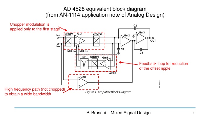
AD 4528 equivalent block diagram (from AN-1114 application note of Analog Design) Chopper modulation is applied only to the first stage Feedback loop for reduction of the offset ripple High frequency path (not chopped) to obtain a wide bandwidth P. Bruschi Mixed Signal Design 1
A recently introduced chopper op-amp Very low offset voltage Note: residual offset and flicker noise shifted at the clock frequency Very low noise density down to low frequencies P. Bruschi Mixed Signal Design 2
Note: relatively high bias currents for a CMOS amplifier: effect of charge injection from the input switches Note: relatively low input resistance (effect of alternating Vin and Vin across the input capacitance) P. Bruschi Mixed Signal Design 3
Finite input resistance of chopper amplifiers Amplifier input capacitance Input modulator = = ( ) 2 Q V V C V C end start in in in Phase 2 V C = 2 Q in in Let us start from phase 1 Phase 1 again V I 1 = = = 4 Q V C (one period) in R tot in in eq 4 C f eq in ck 4 V C = = in T in 4 I V C f = = 2 Q V C 2 Q V C eq in in ck in in in in P. Bruschi Mixed Signal Design 4