Late-Stage IC Implementation Optimization
This study focuses on optimizing scan chain timing during late-stage IC implementation to address issues such as hold violations, dynamic voltage drops, and test time reduction. The methodology, experimental results, and conclusions are presented to highlight the importance of late-stage optimization in improving robustness and reducing overheads in IC design.
Download Presentation

Please find below an Image/Link to download the presentation.
The content on the website is provided AS IS for your information and personal use only. It may not be sold, licensed, or shared on other websites without obtaining consent from the author.If you encounter any issues during the download, it is possible that the publisher has removed the file from their server.
You are allowed to download the files provided on this website for personal or commercial use, subject to the condition that they are used lawfully. All files are the property of their respective owners.
The content on the website is provided AS IS for your information and personal use only. It may not be sold, licensed, or shared on other websites without obtaining consent from the author.
E N D
Presentation Transcript
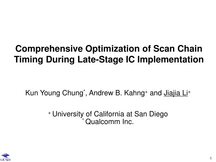
Comprehensive Optimization of Scan Chain Timing During Late-Stage IC Implementation Kun Young Chung*, Andrew B. Kahng+and Jiajia Li+ + University of California at San Diego * Qualcomm Inc. 1
Agenda Motivation Related Works Our Methodology Experimental Results Conclusions 2
Scan Chain Timing Matters Scan chain timing is important to test time, cost and robustness Issues Small number of logic instances along scan timing paths Scan timing paths are vulnerable to hold violations Increase of #hold buffers (area, routing congestion) Scan shift at a high frequency large dynamic voltage drop (DVD) degraded setup scan timing false failure Goals Scan ordering for reduced #hold buffers Gating insertion to minimize timing degradation due to DVD Problems are not new, but do previous approaches really solve these problems? 3
Need Late-Stage Optimization Hold-critical paths and DVD hotspots vary between early (post-placement) and late (post-routing) stages Clock skew and interconnect delay affect hold timing Hold-critical scan timing paths vary Post-placement Post-routing Design: LEON3MP Blue: non-critical paths Red: hold-critical paths 4
Need Late-Stage Optimization Hold-critical paths and DVD hotspots vary between early (post-placement) and late (post-routing) stages Clock buffer insertion and timing optimization during routing affect DVD hotspots Dynamic voltage drop (during scan shift) varies Post-placement Post-routing Design: LEON3MP Switching activity at test input = 50% 5
Need Late-Stage Optimization Hold-critical paths and DVD hotspots vary between early (post-placement) and late (post-routing) stages Clock skew and interconnect delay affect hold timing Clock buffer insertion and timing optimization during routing affect DVD hotspots An early-stage optimization might be misleading Focus onoptimizations during late-stage IC implementation Challenges Consideration of timing impact on datapaths in function mode Minimization of area and power overheads 6
Agenda Motivation Related Works Our Methodology Experimental Results Conclusions 7
Related Works Scan ordering [Feuer83] uses TSP-based heuristic for scan ordering [Gupta03] considers physical information (routing segments) for scan ordering to minimize wirelength [Tudu13] performs test-pattern-aware scan ordering to minimize transitions [Teene03]applies skew-aware scan ordering to minimize #hold buffers Ours also considers wire delay and datapath timing Gating approaches [Gerstend rfer00] inserts gating logic to suppress activity of fanout combinational cells during scan shift [Elshoukry07] avoids gating insertion on timing-critical paths [Jayaram10] proposes to gate internal nodes inside fanout cones of scan cells Ours is the first gating approach for minimization of DVD- aware timing degradation 8
Agenda Motivation Related Works Our Methodology Scan Ordering for Hold Buffer Removal DVD-Aware Gating Insertion Experimental Results Conclusions Post-Routing Scan OrderingGiven a routed design, timing constraints, upper bound on wirelength penalty, perform scan ordering to minimize #hold buffers 9
Causes of Hold Violations Negative clock skew values Skew distribution of scan timing paths with hold buffers Majority of hold-critical paths has negative skew Design: LEON3MP, 28LP Small distance between launch and capture FFs Distances between launch and capture FFs versus hold slacks Smaller distances lead to smaller hold slacks Red: hold slack < 50ps Blue: holdslack < 100ps Green:holdslack < 150ps Design: LEON3MP, 28LP 10
Causes of Hold Violations Negative clock skew values Skew distribution of scan timing paths with hold buffers Majority of hold-critical paths has negative skew Goal: (i) achieve greater incidence of positive skew values, and (ii) slightly increase start-end FF Design: LEON3MP, 28LP Small distance between launch and capture FFs distances Remove hold buffers Distances between launch and capture FFs versus hold slacks Smaller distances lead to smaller hold slacks Red: hold slack < 50ps Blue: holdslack < 100ps Green:holdslack < 150ps Design: LEON3MP, 28LP 11
Scan Ordering for Hold Buffer Removal Scan ordering procedure for each scan chain Ck = original ordering of Ck h = original #hold buffers in Ck for i = 2 to (Nk - 2) // Nk = #scan cells in Ck for j = (i + 1) to (Nk - 1) = 2OptSwap( , i, j) h = #hold buffers with if (h < h && is feasible) then = ; h = h endif endfor endfor Reorder Ck based on endfor feasible = (i) no timing degradation on datapaths, (ii) no additional hold violations, (iii) meet upper bound on wirelength penalty Subchain with fixed ordering is merged into one node before optimization Example of skew-aware scan ordering 12
Agenda Motivation Related Works Our Methodology Scan Ordering for Hold Buffer Removal DVD-Aware Gating Insertion Experimental Results Conclusions DVD Mitigation by Gating Given a routed design, timing constraints, power information, upper bound on area overhead, perform gating insertion to maximize minimum DVD-aware slack 13
Overall Gating Insertion Flow 1. Determine DVD hotspots DVD hotspot = a grid with large DVD Only consider DVD hotspots having impact on scan (setup) timing slacks Worst-DVD hotspot hotspot with largest impact on timing 2. Find gating locations Reduce dynamic power within selected DVD hotspots Minimize number of gating logic insertion 3. ECO-based gating insertion Minimize area, power and wirelength penalties Illustration of gating insertion Gating logic (OR gate) Comb logic cone SE D TI Q D TI Scan timing path Q TE TE 14
DVD-Aware Gating Insertion (1) Integer linear programming-based hotspot selection Given limited number (R) of hotspots Maximize the minimum DVD-aware slack (Smin) Maximize Smin Such that Sj+ ( i i) Smin i L r r R Notations SkOriginal slack of scan timing path i Expected scan cell delay improvement from DVD reduction i Binary indicator of whether DVD on scan cell is improved i Binary indictor of whether DVD hotspot is selected (optimized) L Large constant number 15
DVD-Aware Gating Insertion (2) Netlist traversal to find gating locations Minimize dynamic power within selected hotspots A simplified example 0.5 1 1. Assign gain of 1 to each cell within selected hotspots 2. Propagate gain values from each cell within selected hotspots backwards based on #fanins 3. Select gating location with the maximum gain Selected gating locations 0.75 0.5 + = 1.5 1 0.75 1 Cells in selected hotspots Candidate gating locations ECO optimization Perform matching optimization (Hungarian method) between white spaces and gating logics 16
Agenda Motivation Related Works Our Methodology Experimental Results Conclusions 17
Design of Experiments Technology: 28LP foundry, dual-VT Example of applicable tool chain Synthesis: Synopsys Design Compiler H-2013.03-SP3 Scan chain insertion: Synopsys DFT Compiler H-2013.03-SP3 (maximum length of each chain = 250) P&R: Synopsys IC Compiler I-2013.12-SP1 Signoff timer: Synopsys PrimeTime H-2013.06-SP2 Power analysis: Synopsys PT-PX H-2013.06-SP2 Vectorless DVD analysis: ANSYS RedHawk Testcases Design DES VGA LEON3MP NETCARD Clock period (ns) 0.85 1.1 2 1.8 #Instances 74035 80412 474108 428974 #Scan chains 45 78 445 358 18
Scan Ordering Results Reference: Default SP&R using a commercial tool flow (orig) Remove up to 82% of hold buffers along scan chains Incur negligible timing and wirelength penalties Design Flow orig opt orig opt orig opt orig opt #Hold buffers 1296 (1.00) 487 (0.38) 202 (1.00) 89 (0.44) 25581 (1.00) 4538 (0.18) 30864 (1.00) 26887 (0.87) WNS (ps) TNS (ns) THS (ns) -21 -0.089 -21 -0.081 -6 -0.019 -6 -0.018 30 0 30 0 -4 -0.004 -4 0 Wirelength (mm) 765.9 766.3 3087.9 3089.7 11088 11084 12729 12720 -0.101 -0.121 -1.222 -1.223 -0.734 -0.705 -13.317 -13.304 DES VGA LEON3MP NETCARD 19
Gating Insertion Results Reference: Default SP&R using a commercial tool flow (orig) Achieve up to 58% improvement of DVD-induced slack degradation ( slack) Small number of gating cells < 1% area penalty Worst DVD does not necessarily correspond to worst DVD-aware slack Design Flow slack (ps) WNS (ps) TNS (ns) #Gating cells DVD (mV) Area ( m2) orig 60 (1.00) -21 -0.089 opt 25 (0.42) -21 -0.079 orig 159 (1.00) -6 -0.019 opt 118 (0.74) -6 -0.029 orig 471 (1.00) 30 0 opt 383 (0.81) 30 0 orig 576 (1.00) -4 -0.004 opt 496 (0.86) -8 -0.008 - 85 84 93 82 129 121 163 147 79662 79705 120832 120873 699885 699969 575869 576022 DES 36 - 42 - 62 - 111 VGA LEON3MP NETCARD 20
Agenda Motivation Related Works Our Methodology Experimental Results Conclusions 21
Futures and Conclusions Comprehensive scan timing optimization during late- stage IC implementation Validation with realistic implementation flow (under guidance of our industrial colleagues) Up to 82% hold buffer reduction and 58% improvement of DVD-induced scan timing degradation Future works Co-optimization of gating insertion, scan ordering and test pattern generation DVD optimization during capture stage Predictive model to determine DVD hotspot during scan shift/capture Thanks to Samsung Electronics for research support! 22
THANK YOU ! 23
