Lecture: Memory Basics and Innovations
This lecture covers memory basics and innovations in computer systems, including DRAM main memory, memory architecture, DRAM array access, and organizing ranks, DIMMs, banks, and arrays. Understand how memory is organized, the components involved, and the hierarchy in storage organization.
Download Presentation

Please find below an Image/Link to download the presentation.
The content on the website is provided AS IS for your information and personal use only. It may not be sold, licensed, or shared on other websites without obtaining consent from the author.If you encounter any issues during the download, it is possible that the publisher has removed the file from their server.
You are allowed to download the files provided on this website for personal or commercial use, subject to the condition that they are used lawfully. All files are the property of their respective owners.
The content on the website is provided AS IS for your information and personal use only. It may not be sold, licensed, or shared on other websites without obtaining consent from the author.
E N D
Presentation Transcript
Lecture: Memory Basics and Innovations Topics: memory organization basics, memory scheduling policies 1
DRAM Main Memory Main memory is stored in DRAM cells that have much higher storage density DRAM cells lose their state over time must be refreshed periodically, hence the name Dynamic DRAM access suffers from long access time and high energy overhead 2
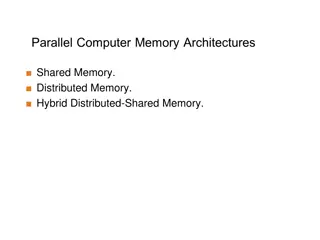
Memory Architecture Bank Row Buffer Processor Memory Controller Address/Cmd DIMM Data DIMM: a PCB with DRAM chips on the back and front Rank: a collection of DRAM chips that work together to respond to a request and keep the data bus full A 64-bit data bus will need 8 x8 DRAM chips or 4 x16 DRAM chips or.. Bank: a subset of a rank that is busy during one request Row buffer: the last row (say, 8 KB) read from a bank, acts like a cache DDR standards 3
DRAM Array Access 16Mb DRAM array = 4096 x 4096 array of bits 12 row address bits arrive first Row Access Strobe (RAS) 4096 bits are read out Some bits returned to CPU 12 column address bits arrive next Column decoder Column Access Strobe (CAS) Row Buffer 4
Organizing a Rank DIMM, rank, bank, array form a hierarchy in the storage organization Because of electrical constraints, only a few DIMMs can be attached to a bus One DIMM can have 1-4 ranks For energy efficiency, use wide-output DRAM chips better to activate only 4 x16 chips per request than 16 x4 chips For high capacity, use narrow-output DRAM chips since the ranks on a channel are limited, capacity per rank is boosted by having 16 x4 2Gb chips than 4 x16 2Gb chips 5
Organizing Banks and Arrays A rank is split into many banks (8-16) to boost parallelism within a rank Ranks and banks offer memory-level parallelism A bank is made up of multiple arrays (subarrays, tiles, mats) To maximize density, arrays within a bank are made large rows are wide row buffers are wide (e.g., 8KB read for a 64B request, called overfetch) 6
Problem 1 What is the maximum memory capacity supported by the following server: 2 processor sockets, each socket has 4 memory channels, each channel supports 2 dual-ranked DIMMs, and x4 4Gb DRAM chips? What is the memory bandwidth available to the server if each memory channel runs at 800 MHz? 7
Problem 1 What is the maximum memory capacity supported by the following server: 2 processor sockets, each socket has 4 memory channels, each channel supports 2 dual-ranked DIMMs, and x4 4Gb DRAM chips? 2 sockets x 4 channels x 2 DIMMs x 2 ranks x 16 chips x 4Gb capacity = 256 GB What is the memory bandwidth available to the server if each memory channel runs at 800 MHz? 2 sockets x 4 channels x 800M (cycles per second) x 2 (DDR, hence 2 transfers per cycle) x 64 (bits per transfer) = 102.4 GB/s 8
Problem 2 A basic memory mat has 512 rows and 512 columns. What is the memory chip capacity if there are 512 mats in a bank, and 8 banks in a chip? 9
Problem 2 A basic memory mat has 512 rows and 512 columns. What is the memory chip capacity if there are 512 mats in a bank, and 8 banks in a chip? Memory chip capacity = 512 rows x 512 cols x 512 mats x 8 banks = 1 Gb 10
Row Buffers Each bank has a single row buffer Row buffers act as a cache within DRAM Row buffer hit: ~20 ns access time (must only move data from row buffer to pins) Empty row buffer access: ~40 ns (must first read arrays, then move data from row buffer to pins) Row buffer conflict: ~60 ns (must first precharge the bitlines, then read new row, then move data to pins) In addition, must wait in the queue (tens of nano-seconds) and incur address/cmd/data transfer delays (~10 ns) 11
Open/Closed Page Policies If an access stream has locality, a row buffer is kept open Row buffer hits are cheap (open-page policy) Row buffer miss is a bank conflict and expensive because precharge is on the critical path If an access stream has little locality, bitlines are precharged immediately after access (close-page policy) Nearly every access is a row buffer miss The precharge is usually not on the critical path Modern memory controller policies lie somewhere between these two extremes (usually proprietary) 12
Problem 3 For the following access stream, estimate the finish times for each access with the following scheduling policies: Req Time of arrival Open Closed Oracular X 0 ns Y 10 ns X+1 100 ns X+2 200 ns Y+1 250 ns X+3 300 ns Note that X, X+1, X+2, X+3 map to the same row and Y, Y+1 map to a different row in the same bank. Ignore bus and queuing latencies. The bank is precharged at the start. 13
Problem 3 For the following access stream, estimate the finish times for each access with the following scheduling policies: Req Time of arrival Open Closed Oracular X 0 ns 40 40 40 Y 10 ns 100 100 100 X+1 100 ns 160 160 160 X+2 200 ns 220 240 220 Y+1 250 ns 310 300 290 X+3 300 ns 370 360 350 Note that X, X+1, X+2, X+3 map to the same row and Y, Y+1 map to a different row in the same bank. Ignore bus and queuing latencies. The bank is precharged at the start. 14
Problem 4 For the following access stream, estimate the finish times for each access with the following scheduling policies: Req Time of arrival Open Closed Oracular X 10 ns X+1 15 ns Y 100 ns Y+1 180 ns X+2 190 ns Y+2 205 ns Note that X, X+1, X+2, X+3 map to the same row and Y, Y+1 map to a different row in the same bank. Ignore bus and queuing latencies. The bank is precharged at the start. 15
Problem 4 For the following access stream, estimate the finish times for each access with the following scheduling policies: Req Time of arrival Open Closed Oracular X 10 ns 50 50 50 X+1 15 ns 70 70 70 Y 100 ns 160 140 140 Y+1 180 ns 200 220 200 X+2 190 ns 260 300 260 (or 285) Y+2 205 ns 320 240 320 (or 225) Note that X, X+1, X+2, X+3 map to the same row and Y, Y+1 map to a different row in the same bank. Ignore bus and queuing latencies. The bank is precharged at the start. ** A more sophisticated oracle can do even better. 16
