Longitudinal Digital Damper for the Fermilab Booster 2020-2025
The Longitudinal Digital Damper for the Fermilab Booster project involves cutting-edge instrumentation and technology. It includes components such as the VME/VXS Digitizer Module, DAC3283 dual 16-bit ADC, ADS62P69 dual 16-bit ADC, and more. The project aims to enhance the performance and control of the Booster Accelerator System for Advanced Studies and Nuclear Energy. Through advanced digital signal processing and data acquisition, this project sets a new standard in dampening longitudinal oscillations for the booster system.
Download Presentation

Please find below an Image/Link to download the presentation.
The content on the website is provided AS IS for your information and personal use only. It may not be sold, licensed, or shared on other websites without obtaining consent from the author.If you encounter any issues during the download, it is possible that the publisher has removed the file from their server.
You are allowed to download the files provided on this website for personal or commercial use, subject to the condition that they are used lawfully. All files are the property of their respective owners.
The content on the website is provided AS IS for your information and personal use only. It may not be sold, licensed, or shared on other websites without obtaining consent from the author.
E N D
Presentation Transcript
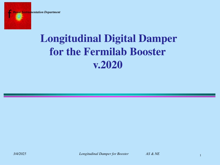
f Beam Instrumentation Department Longitudinal Digital Damper for the Fermilab Booster v.2020 3/4/2025 Longitudinal Damper for Booster AS & NE 1
f Beam Instrumentation Department LDD based on the Generic VME/VXS Digitizer Module : 4 channels, 16 bit Inputs 4 channels, 16 bit Outputs DC/AC- up to 250MSPS Operation Up to 32M samples per channel DDR3 buffer 3/4/2025 Longitudinal Damper for Booster AS & NE 2
f Beam Instrumentation Department BLOCK DIAGRAM To VXS Fabric & To Front ETH GATE TRIGGER ETH 1000-X MAC TCLK External Control SYNC IN VME bus Master/Slave Transfer SYNC OUT VME Drivers Pre-Amps 256MB DDR3 FPGA D A C 4 Analog Outputs 16bit, 250MSPS Cyclone V 5CEFA7F31C8 2x64MB FLASH 4 Analog Inputs 16bit,250MSPS A D C JTAG Base Oscillator ADC s Oscillator ADC s Clock Synthesizer CDCE62005 External Clock 3/4/2025 Longitudinal Damper for Booster AS & NE 3
f Beam Instrumentation Department ADS62P69 Dual, 16 bit, 250MSPS ADC with serial LVDS Outputs Features Maximum Sample rate: 250MHz 16-bit Resolution Analog Input Bandwidth: 900MHz 6 dB Programmable Gain DC Offset Correction 100 dB Cross-Talk 0.820W/per ch at 250 MSPS Serialized LVDS Outputs 3-Wire Serial Digital Interface 3/4/2025 Longitudinal Damper for Booster AS & NE 4
f Beam Instrumentation Department DAC3283 Dual, 16 bit, 250MSPS ADC with serial LVDS Outputs Features Maximum Sample rate: 250MHz 16-bit Resolution 2x,4x FIR Filters Programmable Gain DC Offset Correction 8 bit Input LVDS Data Bus 3-Wire Serial Digital Interface 3/4/2025 Longitudinal Damper for Booster AS & NE 5
f Beam Instrumentation Department 2 Channels 16bit 250 MHz ADC AV_+3V3 AV_+3V3 AV_+3V3 L29 R105 1k IHLP1616BZ-ER-2R2-M01 L30 10uH DV_3V3 L27 10uH L28 10uH DV_1V8 C155 C156 ADC_3V3 ADC_1V8 U39 U40 0u1 0u1 ADA4927-1YCPZ-R2 ADA4927-1YCPZ-R2 R106 1k 5 6 7 8 5 6 7 8 C162 C157 C159 C160 C167 C161 C163 C158 R109 348 Vcc(+5V) Vcc(+5V) R107 348 1 12 1 12 PA_PWDN1 PA_PWDN1 22uF 0u1 0u1 22uF 0u1 -fb -fb 0u1 0u1 0u1 PD PD R111 49.9 R108 165 R110 165 2 11 2 11 Out- Out- In+ In+ + + R114 49.9 3 10 3 10 - - 16 33 34 38 48 58 adc1_pdout[6:0] adc1_ndout[6:0] Out+ Out+ In- In- 1 R112 192 R113 165 4 9 PAD 4 9 PAD ADC_VCM Vocm Vocm AVDD1 AVDD2 AVDD3 DRVDD1 DRVDD2 DRVDD3 DRVDD3 +fb +fb 22 R115 348 R116 348 NC1 Vee(-5V) Vee(-5V) adc2_pdout[6:0] 13 14 15 16 13 14 15 16 AV_-2V5 AV_-2V5 23 Vneg1 adc2_ndout[6:0] VCM 41 adc1_pdout0 DoutA0_p 40 adc1_ndout0 adc1_pdout1 adc1_ndout1 L31 10uH C164 L32 10uH C165 C166 0u1 DoutA0_n 43 DoutA2_p 42 0u1 0u1 DoutA2_n PCB top side 45 adc1_pdout2 adc1_ndout2 DoutA4_p 44 DoutA4_n 47 adc1_pdout3 R117 5 R118 100 DoutA6_p 29 46 pIN_adc1 adc1_ndout3 adc1_pdout4 PCB bottom side T6 INA_p DoutA6_n 51 T7 J5 131-3701-341 DoutA8_p 30 50 nIN_adc1 adc1_ndout4 adc1_pdout5 C168 ADT1-ED9855/1 3 R119 ADT1-ED9855/1 1 R120 INA_n DoutA8_n 53 1 6 4 DoutA10_p 52 adc1_ndout5 49.9 49.9 DoutA10_n 55 adc1_pdout6 5 5 R121 DoutA12_p 54 adc1_ndout6 0u1 C169 DoutA12_n 2 3 4 5 1 4 6 3 49.9 R122 R123 R124 100 19 61 60 63 62 3 2 5 4 7 6 9 8 11 10 pIN_adc2 adc2_pdout0 0u1 INB_p DoutB0_p DoutB0_n DoutB2_p DoutB2_n DoutB4_p DoutB4_n DoutB6_p DoutB6_n DoutB8_p DoutB8_n DoutB10_p DoutB10_n DoutB12_p DoutB12_n adc2_ndout0 adc2_pdout1 adc2_ndout1 49.9 49.9 20 nIN_adc2 R125 5 U41 INB_n adc2_pdout2 adc2_ndout2 ADS62P49IRGCT C170 0u1 25 adc2_pdout3 adc_pCLK adc_nCLK CLK_p 26 adc2_ndout3 adc2_pdout4 CLK_n AV_+3V3 C171 0u1 adc2_ndout4 adc2_pdout5 12 SReset SDOUT SReset 64 adc2_ndout5 R126 1k SDOUT 14 adc2_pdout6 AV_+3V3 AV_+3V3 SDATA SDATA 13 15 adc2_ndout6 SCLK SCS SCLK SEN L33 10uH L34 10uH 57 C172 C173 adc_pDCO DCLK_p 56 U42 U43 R127 1k adc_nDCO 0u1 0u1 DCLK_n ADA4927-1YCPZ-R2 ADA4927-1YCPZ-R2 35 5 6 7 8 5 6 7 8 CTRL1 36 37 R131 348 CTRL2 CTRL3 Vcc(+5V) Vcc(+5V) R130 348 1 12 1 12 PA_PWDN2 PA_PWDN2 -fb -fb PD PD R128 165 R129 165 R132 R135 49.9 49.9 2 11 2 11 DRGND1 DRGND1 DRGND2 Out- Out- In+ In+ TPAD10 TPAD11 TPAD12 TPAD13 TPAD14 TPAD15 TPAD16 + + AGND1 AGND2 AGND3 AGND4 AGND5 AGND6 AGND7 AGND8 TPAD1 TPAD2 TPAD3 TPAD4 TPAD5 TPAD6 TPAD7 TPAD8 TPAD9 3 10 3 10 - - Out+ Out+ In- In- R133 192 R134 165 4 9 PAD 4 9 PAD ADC_VCM Vocm Vocm 17 18 21 24 27 28 31 32 65 66 67 68 69 70 71 72 73 74 75 76 77 78 79 80 39 49 59 +fb +fb R136 348 R137 348 Vee(-5V) Vee(-5V) 13 14 15 16 13 14 15 16 AV_-2V5 AV_-2V5 L35 10uH C174 L36 10uH C175 0u1 0u1 PCB top side R138 5 PCB bottom side T9 T8 J4 131-3701-341 ADT1-ED9855/1 1 C176 ADT1-ED9855/1 3 R139 R140 4 1 6 49.9 49.9 5 Item No. Part No. Description or Size Qty. Req. 5 R141 0u1 C177 6 3 2 3 4 5 1 4 49.9 R142 R143 Parts List 0u1 49.9 49.9 R144 5 Unless Otherwise Specified Originator A.Semenov 11.16.2009 Fractions Decimals Angles Drawn A.Semenov 11.16.2009 + - + - + - Checked P.Prieto 11.17.2009 Approved M.Wend 11.18.2009 1. Break all sharp edges 1/64" maximum. 2. Do not scale drawing. 3. Dimensioning in accord with ANSI Y14.5 standards. Used On Max. all machined surfaces Material f FERMI NATIONAL ACCELERATOR LABORATORY UNITED STATES DEPARTMENT OF ENERGY Instr VME 12ch 14bit 250MHz Digitizer 2 channels 14bit 250MHz ADC's Schematic Scale Software Drawing Number 0880-ED-417142 Rev 4 OrCAD Capture Version 10.3.0 Date: Saturday, January 07, 2012 Sheet 2 of 61 3/4/2025 Longitudinal Damper for Booster AS & NE 6
f Beam Instrumentation Department ADC s Clock Synthesizer and Distribution Stage CDCE62005: Additive output jitter 1ps RMS Input reference frequencies to 1500MHz Output frequency ranges from 4.25MHz to 1.175GHz in Synthesizer Mode Output frequency ranges up to 1.5GHz in Fun-out Mode Wide Tuning Range 1.750 GHZ-2.356 GHZ Fine delay adjust for output Serial mode control port 3/4/2025 Longitudinal Damper for Booster AS & NE 7
FPGA Design f Beam Instrumentation Department Data from ADC s ADC Data LVDS Receiver NIOS II DDR3 2x 64Mx16 LDD 16 Harmonics (I,Q) Data To DAC s FLASH 64Mbit DAC s Data LVDS Transmitter QSYS Interconnect Fabric VME BUS VME interface DSP VXS, Ethernet TCLK ETH 1000-X MAC Digitizer SYNC Module Gate Trigger Sync RemUpdate Core DCDC Converters To ADC s DCDC frequency control ADC & Clock SPI To Clock Station 3/4/2025 Longitudinal Damper for Booster AS & NE 8
Longitudinal Digital Damper FPGA Design v.2020 f Beam Instrumentation Department DUC DDC 16 ch Mixer IQ IIR & M,Phi Tuner N = 16 N = 16 Mixer DUC #15 DDC #15 DUC #0 2 DDC #0 6 7 Complex Multiplier Mode s mask 1 3 5 4 8 Beam 38-90MHz IIR FIR 2 Order, FP ADC 14bit, 250MHz CIC 0.5*RF cos CIC 0.5*RF Cos NCO s Sin Feedback NCO s sin 7 6 +/- 2 LSB/USB Line M & Phi RAM RF 38-53MHz PLL 4xRF to RF 4096Words (32bit) Feedback DAC 0 Cavity [I(16bit) + Q(16bit)] x 16ch x 256points MIX VSA Vectors TCLK Sync To VSA Input Feedback DAC 1 MIX VSA Vectors VSA Tests Check Point: DMA => RAM 1 3/4/2025 Longitudinal Damper for Booster AS & NE 9
Longitudinal Digital Damper FPGA Design v.2020 f Beam Instrumentation Department IQ 16 ch Mixer IIR & M,Phi Tuner DDC DUC Mixer DUC #0 2 DDC #0 6 7 Complex Multiplier Mode s mask 1 3 5 4 8 Beam 38-90MHz IIR FIR 2 Order, FP ADC 14bit, 250MHz CIC 0.5*RF cos CIC 0.5*RF Cos NCO s Sin Feedback NCO s sin 7 6 RF +/- 52.0-53MHz 2 LSB/USB Line PLL 4xRF M & Phi RAM 3/4/2025 Longitudinal Damper for Booster AS & NE 10
Longitudinal Digital Damper IIR & MPhase Tuner. f Beam Instrumentation Department IIR 2 order filter math: y(n) = [b0*x(n)+b1*x(n-1)+b2*x(n-2)+b3*x(n-3)]/[1+a0*y(n-1)+a1*y(n-2)] or, s(n) = x(n) - a1*s(n-1) - a2*s(n-2) , y(n) = b0*s(n) + b1*s(n-1) + b2*s(n-2) , x(n) - input samples (I &Q), s(n) - intermediate signal, y(n) - output samples (I &Q) M & Phase Tuner, FP IIR FIR 2 Order, FP y(n) = b0*s(n) + b1*s(n-1) + b2*s(n-2) s(n) = x(n) - a1*s(n-1) - a2*s(n-2) Complex Multiplier, FP From DDC CIC 0.5*RF, X(n), I/Q 32bits b0 5 4 To DUC CIC 0.5*RF, X(n), I/Q 32bits S(n-1) FP to 32bit b1 a0 Line S(n-2) M & Phi RAM b2 a1 4096Words (32bit) [I(16bit) + Q(16bit)] x 16ch x 256points 1 3/4/2025 Longitudinal Damper for Booster AS & NE 11
