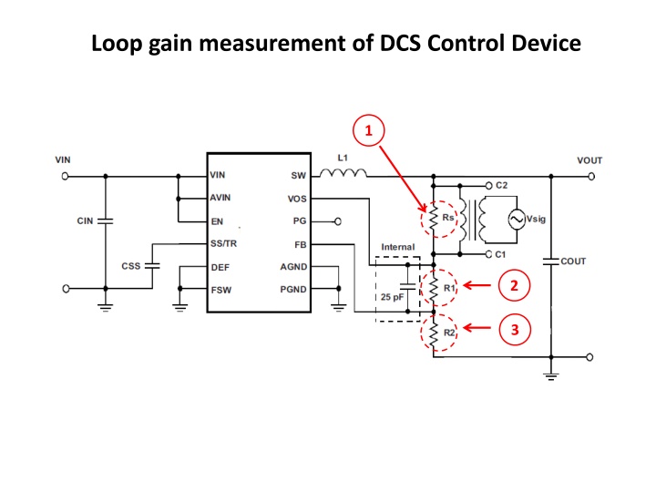
Loop gain measurement of DCS Control Device
This collection features images and comments related to loop gain measurement of DCS control devices, specifically focusing on TLV62090 voltage outputs at different input voltages. The images depict circuit layouts and provide insights such as the importance of avoiding interference between certain lines to minimize switching noise. Explore these visuals for a better understanding of optimizing control device performance.
Download Presentation

Please find below an Image/Link to download the presentation.
The content on the website is provided AS IS for your information and personal use only. It may not be sold, licensed, or shared on other websites without obtaining consent from the author.If you encounter any issues during the download, it is possible that the publisher has removed the file from their server.
You are allowed to download the files provided on this website for personal or commercial use, subject to the condition that they are used lawfully. All files are the property of their respective owners.
The content on the website is provided AS IS for your information and personal use only. It may not be sold, licensed, or shared on other websites without obtaining consent from the author.
E N D
Presentation Transcript
1.TLV62090 3.3Vout @ 5VIN #1 + #3 Layers overlap #1 Layer PVIN AVIN PVIN SS CN CP AGND FB EN PGND PGND VOS DEF SW SW PG
1.TLV62090 3.3Vout @ 5VIN #1 + #3 Layers overlap My comment is *FB line should avoid SW area due to switching noise
2.TLV62090 1.8Vout @ 5VIN #1 + #3 Layers overlap #1 Layer PVIN PVIN AVIN SS EN CN CP AGND FB PGND PGND VOS DEF PG SW SW
2.TLV62090 1.8Vout @ 5VIN #1 + #3 Layers overlap My comment is *FB line should avoid SW area due to switching noise *PG line can short
3.TLV62090 1.5Vout @ 5VIN #1 Layer #1 + #3 Layers overlap AVIN PVIN PVIN SS CN CP EN PGND PGND AGND FB VOS DEF SW SW PG
3.TLV62090 1.5Vout @ 5VIN #1 + #3 Layers overlap My comment is *Nothing especially Is there any comment?
