Explore the intricate details of memory organization in microprocessor-based system design, including address space allocation, asynchronous data transfers, and control signals. Learn about the physical organization of memory, interrupt vector tables, and the utilization of function codes for memory space segmentation.
Please find below an Image/Link to download the presentation.
The content on the website is provided AS IS for your information and personal use only. It may not be sold, licensed, or shared on other websites without obtaining consent from the author. If you encounter any issues during the download, it is possible that the publisher has removed the file from their server.
You are allowed to download the files provided on this website for personal or commercial use, subject to the condition that they are used lawfully. All files are the property of their respective owners.
The content on the website is provided AS IS for your information and personal use only. It may not be sold, licensed, or shared on other websites without obtaining consent from the author.
E N D
Presentation Transcript
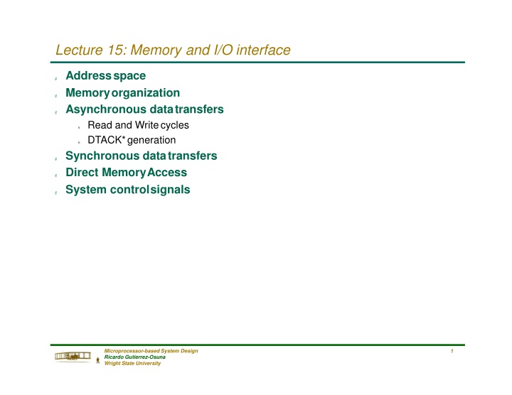
Lecture 15: Memory and I/O interface g Addressspace g Memoryorganization g Asynchronous datatransfers Read and Writecycles n DTACK*generation n g Synchronous datatransfers g Direct MemoryAccess g System controlsignals Microprocessor-based System Design Ricardo Gutierrez-Osuna Wright State University 1
Address space g The address bus of the 68000 consists of 23 independent address lines A0-A23 n Since the data bus is 16-bit wide, we have an address space of 8M words g Two additional control lines are used to select individual bytes n Upper Data Strobe (UDS*) n Lower Data Strobe (LDS*) g UDS* and LDS* are used to enable byte-wide upper and lower data banks n Upper data banks are selected by UDS* and contain data bits D8-D15 n Lower data banks are selected by LDS* and contain data bits D0-D7 g A01-A23 are shared by the two data banks and are used to address individual bytes within each bank g This physical organization of memory explains why words must be stored at even memory addresses Microprocessor-based System Design Ricardo Gutierrez-Osuna Wright State University 2
Memory organization g Dedicated and general use memory 00000016 Exception vectortable Memory locations 000000 to 0003FE have a dedicated function: 0003FE16 00040016 n g storage of the interrupt vectortable The rest of the memory space is for general use, it can be used to store data, instructions or address information n Generaluse memory g Three additional output pins on the 68000, the function code (FC0-FC2), indicate whether the bus cycle is FFFFFE16 accessing data or program instructions n being executed in user or supervisor mode n Function code FC2 0 0 0 0 1 1 1 1 Reference class FC1 0 0 1 1 0 0 1 1 FC0 0 1 0 1 0 1 0 1 g By using (FC0-FC2), the memory space can be further divided into User programsegment (Unassigned) User data Userprogram (Unassigned) (Unassigned) Supervisor data Supervisorprogram Interrupt Acknowledge n User data segment n Supervisor programsegment n Supervisor data segment n g As an example, (FC0-FC2) are decoded and used to assert the appropriate chip select (CS*) signals Microprocessor-based System Design Ricardo Gutierrez-Osuna Wright State University 3
Asynchronous memory and I/O interface g Asynchronous means that n once a bus cycle is initiated to read or write instructions or data, it is not completed until a response is provided by the memory or I/O subsystem n This response is an acknowledgement signal that tells the 68000 that the current bus cycle is compete g The basic asynchronous operation is n The 68000 puts an address on the address bus and asserts Address Strobe (AS*) to signal memory and I/O devices that a valid address information is available on the bus n The memory or I/O device asserts Data Transfer Acknowledge (DTACK*) to signal the 68000 that g valid data is available on the data bus during a read operation (the 68000 latches data when DTACK* is asserted) g data has been successfully written to the memory or I/O device g Asynchronous operation allows the 68000 to interface with slow memories or I/O devices Microprocessor-based System Design Ricardo Gutierrez-Osuna Wright State University 4
READ cycle flowchart g An asynchronous read cycle is characterized by the interlocked handshaking procedure that takes place between Bus master Bus slave Address the slave 1. Set R/W* toread 2. Place function code on FC0-FC2 3. Place address on A01-A23 4. Assert address strobe AS* 5. Assert UDS* and LDS* n the bus master (CPU) and n the bus slave (memory or I/O device) g The following steps take place n The CPU indicates its intentions by Output the data g forcing R/W* HIGH and 1. Decode the address 2. Place data on D0-D15 3. Assert DTACK* g setting up an address g asserting AS*, UDS* and LDS* n The slave detects that AS*, UDS* and LDS* are asserted and then Acquire the data 1. Latch data 2. Negate UDS* and LDS* 3. Negate address strobe AS* g places data on the data bus g asserts DTACK* n Upon DTACK* assertion, the CPU g latches data from data bus Terminate the cycle g Negates AS*, UDS* and LDS* 1. Remove data from D0-D15 2. Negate DTACK* n Upon negation of AS*, UDS* and LDS*, the slave g removes data from data bus Start the next cycle g Negates DTACK* n At this point we can start a new bus cycle Microprocessor-based System Design Ricardo Gutierrez-Osuna Wright State University 5
READ cycle timing diagram g Each bus cycle consists of a minimum of 4 clock cycles, divided into eight states S0-S7 A bus cycle starts in state S0 with the clock high and ends in state S7 with the clocklow n This basic cycle can be extended by the insertion of wait states between S4 and S5 g Narrative n During S0 all signals are negated with the exception of R/W*, which becomes high to indicate a read operation n In state S1, the address on A01-A23 becomes valid and remains so until state S0 of next cycle In state S2 the address strobe AS* goes active- low, indicating that the contents of the address bus are valid At the same time, UDS* and LDS* go active-low and initiate the memoryaccess At the end of S4, the CPU tests DTACK* g If DTACK* is inactive, the CPU inserts wait states between S4 and S5 until DTACK* goes active-low on the falling edge of S4 During S7, the CPU g negates AS*, UDS* andLDS* g latches the datainternally The negation of the 3 strobes causes the memory to g return its data output pins to high impedance (floating) state g negate DTACK* n n n n n n Microprocessor-based System Design Ricardo Gutierrez-Osuna Wright State University 6
WRITE cycle flowchart g The asynchronous write cycle is very similar to the read cycle we saw before Bus master Bus slave g There are two differences Address the slave 1. Place function code on FC0-FC2 2. Place address on A01-A23 3. Assert address strobe AS* 4. Set R/W* to write 5. Place data on D00-D15 6. Assert UDS* and LDS* n The CPU provides data at the start of the write cycle n The bus slave reads this data Input the data 1. Decode address A01-A23 2. Store data from D00-D15 3. Assert DTACK* Acquire the data 1. Negate UDS* and LDS* 2. Negate address strobe AS* 3. Remove data from D00-D15 4. Set R/W* toread Terminate the cycle 1. Negate DTACK* Start the next cycle Microprocessor-based System Design Ricardo Gutierrez-Osuna Wright State University 7
WRITE cycle timing diagram g Narrative n At the start of a cycle, an address is placed on the address bus A01-A23and g AS* is asserted and R/W* set to logic 0 n After R/W* has set low to indicate a write cycle, the CPU places data on the data bus n Once the contents of the data bus have stabilized, UDS* and LDS* are asserted (approximately 1 cycle after AS* assertion) g This allows the memory to use UDS* and LDS* to latch data from thebus n If DTACK* is asserted before the falling edge of S4, the write cycle is terminated normally g Otherwise wait states are inserted until DTACK* is asserted n At the end of the write cycle g AS*, UDS* and LDS* are negated simultaneously g R/W* is set high g data bus is floated Microprocessor-based System Design Ricardo Gutierrez-Osuna Wright State University 8
DTACK* generation g In the previous slides we assumed that DTACK* was generated by the memory block n This is true for I/O devices such as the 68230 PI/T or the 68681 DUART, which support asynchronous data transfers and have a DTACK* output pin n For devices that do not have this facility (such as memory ICs), the DTACK* signal must be generated by the systems designer with additional circuitry g The circuit below can be used to generate the DTACK* signal with different delays depending on the speed of the device that is being accessed n QA can be used for devices that can operate at maximum (no-wait-state) bus speed n QB can be used to delay DTACK* for one wait state (it will be set on the second rising edge of the clock) n QC can be used to delay DTACK* for two wait states, and so on... CLR AS* Shift register System clock QA QB QCQD Wait states: 0 1 2 3 Jumpers Fast memory From address decoder DTACK* Medium memory Slowmemory Microprocessor-based System Design Ricardo Gutierrez-Osuna Wright State University 9
Synchronous memory and I/O interface g Synchronous bus operation is provided in order to interface slower 8-bit peripherals as those in the 6800 family g This interface is similar to the asynchronous interface except for DTACK* is NOT used Instead, three synchronous bus control signals are used: g Valid Peripheral Address (VPA*) g Valid Memory Address (VMA*) g Enable(E) g Valid Peripheral Address (VPA*) n n When a synchronous peripheral detects that it is being accessed, it asserts VPA* to request a synchronous bus cycle n When the CPU detects that VPA* has been asserted, it initiates the synchronous transfer by means of VMA* and E g Valid Memory Address (VMA*) The CPU asserts VMA* to indicate the peripheral that there is a valid address on the address bus The assertion of VMA* is a response of the CPU to the peripheral s assertion of VPA* g Enable (E) A CPU output derived from the 68000 clock cycle One E cycle is equal to 10 CPU cycles n n n n n E clock is non-symmetric it is low for 6 clock cycles and high for 4 clock cycles n Microprocessor-based System Design Ricardo Gutierrez-Osuna Wright State University 10
Synchronous transfer g Sequence of operations (not detailed) Bus master Bus slave n During state S0, the CPU generates the function codes FC0-FC2 Initiate cycle 1. CPU starts a normal Read or Writecycle n During S1, the CPU puts a valid address on the address bus Define M6800 cycle n When the address is stable in S2 1. External hardware asserts VPA* g AS* is asserted and R/W* set to 1 for a read or 0 for a write g If a write operation is performed, the data is output on D0-D15 and maintained valid for the rest of the bus cycle Synchronize with Enable 1. CPU monitors Enable (E) until it goes low 2. CPU asserts VMA* n By the end of S4, external circuitry must have decoded the address on the bus Transfer data g At this time, it asserts VPA* 1. Slave waits until E is active and then transfers the data n In response to the VPA* assertion, the CPU synchronizes with falling edge of E and then asserts VMA* g This signals the peripheral that a valid address is on the address bus Terminate cycle 1. CPU waits until E goes low (on a Read cycle data is latched as E goes low internally) 2. CPU negates VMA* 3. CPU negates AS*, UDS* and LDS* n The peripheral transfers data on the next rising edge of E g For a read cycle the CPU latches the data on the next falling edge of E n At this point the data transfer is complete and the CPU negates VMA*, AS*, UDS* and LDS* Start next cycle Microprocessor-based System Design Ricardo Gutierrez-Osuna Wright State University 11
Direct Memory Access (DMA) g DMA is a process in which a device (slave) requests the use of the master s buses (address, data and control) for its own use n In a microprocessor-based system, the master is usually the CPU g Once the slave device has control of the bus, it can read or write to the system memory as necessary. When the slave device is finished, it releases control of the master s buses, and the system returns to normal g DMA is used to achieve faster data transfer rates than those attainable with the CPU g To perform DMA on the 68000, three signals are used n Bus Request (BR*) n Bus Grant (BG*) n Bus Grant Acknowledge (BGACK*) Microprocessor-based System Design Ricardo Gutierrez-Osuna Wright State University 12
Why is DMA faster? g Consider the problem of writing a block of memory to an output port, one byte at a time. The following tasks must be performed n Initialize memory and output port addresses n Repeat until all bytes are transferred: g Read byte from memory g Write byte to output port g Increment memoryaddress g Check to see if all bytes transferred g Wait until output port ready for next byte g With this approach, only a fraction of the memory cycles are used for the actual data transfer n the speed of the data transfer is much less than the maximum rate at which data can be read from the memory g DMA is performed with a device called DMA controller (DMAC), which can be thought of a very specialized microprocessor, except for n unlike a data transfer performed by the CPU, no instructions need to be fetched during the transfer to tell the DMAC how to perform the transfer n thus, all memory cycles are available for transferring data Microprocessor-based System Design Ricardo Gutierrez-Osuna Wright State University 13
DMAC operation g A DMA transfer takes place in several stages n Like with any other memory-mapped peripheral, the CPU first sets up the DMAC s registers to define g the quantity of data to be moved g the type of DMA operation g the direction of datatransfer n The DMAC is activated by a request for service from its associated peripheral g When the peripheral asserts REQ*, the DMAC requests control of the bus by asserting its BR*output waiting for a BG* response from the busmaster assertingBGACK* n n n n Once the DMAC has control of the bus, it generates all timing signals needed to transfer data between peripheral and memory n DMA transfers take place in one of two modes g Burst mode: several operands are transferred in consecutive bus cycles g Cycle stealing mode: the DMA relinquishes the system bus between successive data transfers allowing normal CPU processing to be interleaved Microprocessor-based System Design Ricardo Gutierrez-Osuna Wright State University 14
MC6800 pinout We havealready studied all the pins except for these three Microprocessor-based System Design Ricardo Gutierrez-Osuna Wright State University 15
System control pins g Bus Error (BERR*) n When asserted, it indicates that something has gone wrong with the current bus cycle n For example, an access to an invalid memory address is generated by faulty software g The external logic detects this error and asserts BERR* to inform the 68000 n The action taken by the 68000 when it recognizes BERR* is rather complex and depends on the state of HALT*. For simplicity we will state that it will either g try to rerun the faulty cycle or g will generate an exception, and the OS will deal with the bus error g Halt (HALT*) n This I/O pin can be used for three purposes g Used as an input: to force the 6800 to execute one cycle at a time (for debugging purposes) g Used as an input: to rerun a failed bus cycle (see BERR*) g Used as an output: when the 68000 finds itself in a situation it cannot recover from, it stops further processing and asserts HATL* to indicate this situation g Reset (RESET*) n Used as an input: the 68000 loads the SSP from M[$000000] and PC from M[$000004] g The RESET* pin will be connected to the system s hardware reset button n Used as an output: when the processor executes the RESET command, it will assert RESET* pin to reset all external devices g This command does not affect the internal state of the 68000, so it allows peripherals to be reset without resetting the CPU Microprocessor-based System Design Ricardo Gutierrez-Osuna Wright State University 16


")