Memory and I/O Interfacing in Computer Systems
Explore the fundamentals of memory and I/O interfacing in computer systems, including memory structure, requirements, and the interaction between different components. Learn about registers, addressing, data storage, and the types of memory used in computer architecture.

Uploaded on | 3 Views
Download Presentation

Please find below an Image/Link to download the presentation.
The content on the website is provided AS IS for your information and personal use only. It may not be sold, licensed, or shared on other websites without obtaining consent from the author. If you encounter any issues during the download, it is possible that the publisher has removed the file from their server.
You are allowed to download the files provided on this website for personal or commercial use, subject to the condition that they are used lawfully. All files are the property of their respective owners.
The content on the website is provided AS IS for your information and personal use only. It may not be sold, licensed, or shared on other websites without obtaining consent from the author.
E N D
Presentation Transcript
Interfacing Memory Interfacing 1
Outline Interfacing Memory Interfacing I/O Interfacing I/O mapped I/O Memory mapped I/O Memory Interfacing 2
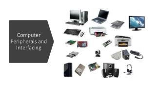
Interface An interface is a medium through which two separate components system exchange information or interact with each other. The between software, hardware, peripheral devices, humans and combinations of these. 1. Memory Interfacing 2. I/O Interfacing of a computer exchange can computer be Memory Interfacing 3
Memory Interfacing Memory is made up of registers. Each register in the memory is one storage location. Each location is identified by an address. Each register consists of storage elements (flip flops) and element stores one bit of data. A storage element is called cell.The data stored in a memory by a process is called writing and are retrieved from the memory by a process is called reading. Memory Interfacing 4
Memory structure and its requirements The read / write memories consist of an array of registers in which each register has unique address. The size of memory is N * M as shown in figures. Memory Interfacing 5
Where N is number of register and M is the word length, in number of bits. As shown in Figure (a) memory chip has 11 address lines Ao A10, one chip select (CS), and two control lines, Read (RD) to enable output buffer and Write (WR) to enable the input buffer. The internal decoder is used to decoder the address lines. Memory Interfacing 8
Figure (b) shows the logic diagram of a typical EPROM (Erasable Programmable Read-Only Memory) with 4096 (4K) register. It has 12 address lines Ao A11, one chip select (CS), one read control signal. Since EPROM does not require the (WR) signal. EPROM (or EPROMs) is used as a program memory and RAM (or RAMs) as a data memory. Memory Interfacing 9
The following table summarize the memory capacity and address lines required for memory interfacing. Memory Interfacing 10
74LS138 (Decoder / Demultiplexer) A decoder is a logic circuit that accepts a set of inputs that represents a binary number and activates only the output that corresponds to the input number. In other words, a decoder circuit looks at its inputs, determines which binary number is present there, and activates the one output that corresponds to that number ; all other outputs remain inactive. Memory Interfacing 11
In its general form, a decoder has N input lines to handle N bits and form one to 2 N output lines to indicate the presence of one or more N-bit combinations. The following figure shows the block diagram of Decoder. Memory Interfacing 12
The LS138 is a high speed 1-of-8 Decoder (3 to 8 decoder). It could also be called a binary- octal decoder or converters because it takes a three bit binary input code and activates the one of the eight outputs corresponding to that code. It is also referred to as a 1-of-8 decoder, because only 1 of the 8 outputs is activated at one time. The pin diagram and the truth table of decoder is shown in the below figures. Memory Interfacing 13
Basic concepts in Memory Interfacing 8085 access 64 Kbytes memory since its address bus is 16-bit. It s not compulsory to use full 64 Kbytes address space. The total memory depends upon the applications. Usually EPROM is used as a program memory and RAM used as a data memory. Number of EPROM and RAM is depends on requirement of applications. Memory Interfacing 16
Microprocessor can communicate (read / write) with only one device at a time. Since the data, address and control buses are common for all the devices. Decoding is necessary to communicate with devices (Memory / I/O). The common address decoding techniques are: Absolute decoding Linear decoding Memory Interfacing 17
Absolute Decoding In the absolute decoding technique the memory chip is selected only for the specified logic level on the address lines: no other logic levels can select the chip. Below figure the memory interface with absolute decoding. Two 8K EPROMs (2764) are used to provide even and odd memory banks. Control signals BHE and Ao are use to enable output of odd and even memory banks respectively. As each memory chip has 8K memory locations, thirteen address lines are required to address each locations, independently. All remaining address lines are used to generate an unique chip select signal. This address technique is normally used in large memory systems. Memory Interfacing 18
Linear Decoding : In small system hardware for the decoding logic can be eliminated by using only required number of addressing lines (not all). Other lines are simple ignored. This technique is referred as linear decoding or partial decoding. The address line A15 is used to select the chips. When A15 is low, EPROM is selected, otherwise RAM gets selected. This technique reduces the cost of decoding circuit, but it has drawback of multiple addresses. Memory Interfacing 20
The above figure shows the addressing of RAM with linear decoding technique. EPROM is selected when A15 line is high and RAM is selected when it is low. The status of other select lines are not considered, since those address lines are not used for generation of chip select signals. Memory Interfacing 22
I/O INTERFACING Microprocessor based system requires the transfer of data between external circuitry to the microprocessor and microprocessor to the external circuitry. User can give information to the microprocessor based system using keyboard, joystick and mouse. User can see the result from the microprocessor with the help of output devices like printer. The transfer of data between microprocessor is called input data transfer, the transfer of data between microprocessor and display device is called Output data transfer. This data transfer is done with the help of I/O ports. keyboard and Memory Interfacing 23
Input Port The input device is connected to the microprocessor through buffer. The simplest form of a input port is a buffer as shown in the figure. This buffer is a tri-state buffer and its output is available only when enable signal is active. When microprocessor wants to read data from the input device (keyboard), the control signals from the microprocessor activates the buffer by asserting enable input of the buffer. Once the buffer is enabled, data from the device is available on the data bus. Microprocessor reads this data by initiating read command. Memory Interfacing 24
Output Port It is used to send the data to the output device such as display from the microprocessor. The simplest form of the output port is a latch. The output device is connected to the microprocessor through latch as shown in the figure. When microprocessor wants to send data to the output device it puts the data on the data bus and activates the clock signal of the latch, latching the data from the data bus at the output of latch. It is then available at the output of latch for the output device. Memory Interfacing 26
Difference between Latch and Buffer A latch is a digital IC which holds the data put into it, 1 or 0, until cleared. A buffer is either analog or digital, and it increases the power of the input signal without changing the value. Memory Interfacing 27
I/O Interfacing I/O interfacing techniques in 8086 In 8086, the control signal IO/M* is used to activate I/O operation. When the control signal is high, it initiates I/O operation. When it s low, it initiates the memory operation. I/O devices can be interfaced to an 8086 in two ways. 1. I/O mapped I/O 2. Memory mapped I/O Memory Interfacing 28
1. I/O Mapped I/O The 8086 has IN and OUT instructions for I/O data transfer. It places I/O device address (port number) on the demultiplexed low order address bus and high order address bus while executing IN and OUT instructions. 8086 needs device address or port number when interfacing I/O devices. 8086 can communicate with 256 different I/O devices. The IN instruction inputs data from an input device into the accumulator and the instructions OUT sends the contents of the accumulator to an output device. These instructions are two byte instructions. The second byte of the instruction specifies the port number and it can be any one of the 256 different I/O devices (00 H to FFH). Memory Interfacing 29
I/O Device selection 8086 gives 8 bit I/O address to select one of the 256 I/O ports. The following steps are used to select I/O device. Decode the address to generate unique signal corresponding to the device address on the bus. When device address signal and control signal (IOR or IOW) both are low, generate device select signal. Use device select signal to activate the interfacing device (I/O port). Memory Interfacing 30
The following figure shows the absolute decoding circuit for the I/O device. The along with OR gates is used to generate device select signal. In this example to generate Y0 low, the address on the address bus is given below: Absolute decoding circuit for the I/O device A2 A1 A0 = 000 H A3 A4 A5 A6 = 0000 H - Makes G1* and G2* low to enable output of decoder A7 = 1H - G is high to enable output of decoder. Therefore the address of the I/O device is 80 H. 3:8 decoder - Activate Y0 output Memory Interfacing 31
2.Memory Mapped I/0 In this method, I/O devices are identified by 16 bit addresses. I/O device becomes a part of the system s memory map. The source and destination register of the data is limited with I/O mapped I/O, because the destination and source register is always accumulator in IN and OUT instructions respectively.But in the case of memory mapped I/O, there are number of source and destinations. MOV r, M Input from a port to specified register MOV M, r Outputs specified register contents to the port. Memory Interfacing 34
Difference between Memory mapped I/O and I/O mapped I/O Memory Interfacing 35
Expected Questions Two Marks Questions K1 Level What is interfacing? Why interfacing is needed? Show the logic diagram of ROM and RAM. What is Memory Interfacing ? What is I/O Interfacing? Memory Interfacing 36
Expected Questions Two Marks Questions K2 Level Compare Memory Interfacing and I/O interfacing. Compare Memory Mapped I/O and I/O mapped I/O. Compare Absolute and Linear decoding. Summarize about input buffer and output Latch. Memory Interfacing 37
Descriptive Questions K2 Level 1. Explain in detail about Memory and I/O interfacing. 2. Demonstrate Memory and I/O Interfacing with neat diagram. 3. Classify the Interfacing. Memory Interfacing 38


 shows the logic diagram of a typical")

")