Memory Hierarchy: Enhancements from Cache to Virtual Memory
Delve into the intricate workings of memory hierarchy, exploring the evolution and improvements in cache memory and virtual memory systems. Discover the significance of memory hierarchy in optimizing processor speed and efficiency, with insights into the ARM Cortex-A53 memory hierarchy.

Download Presentation

Please find below an Image/Link to download the presentation.
The content on the website is provided AS IS for your information and personal use only. It may not be sold, licensed, or shared on other websites without obtaining consent from the author. If you encounter any issues during the download, it is possible that the publisher has removed the file from their server.
You are allowed to download the files provided on this website for personal or commercial use, subject to the condition that they are used lawfully. All files are the property of their respective owners.
The content on the website is provided AS IS for your information and personal use only. It may not be sold, licensed, or shared on other websites without obtaining consent from the author.
E N D
Presentation Transcript
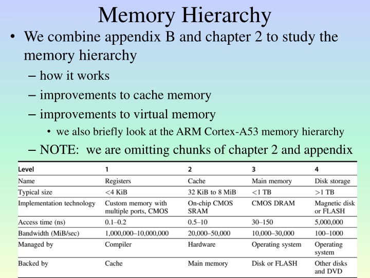
Memory Hierarchy We combine appendix B and chapter 2 to study the memory hierarchy how it works improvements to cache memory improvements to virtual memory we also briefly look at the ARM Cortex-A53 memory hierarchy NOTE: we are omitting chunks of chapter 2 and appendix B
The Memory Problem Significant improvements in processor speed doubling every couple of years (until around 2005, but still increasing from 2005 through 2018) DRAM access times increased mostly linearly since 1980 every year processor speed increases >> DRAM access time since the processor accesses memory in every fetch-execute cycle, there is no sense increasing clock speed unless we find a faster form of memory This is why we use cache memory and create the memory hierarchy
Cache Typical memory hierarchy layout for (a) mobile computers (b) laptop/desktops (c) servers
Performance Formulae CPU execution time must factor in stalls from memory access assume L1 cache responds within the amount of time allotted for the load/store/instruction fetch stage e.g., 1 cycle CPU time = IC * CPI * Clock cycle time CPI = ideal CPI + stalls stalls from both hazards and memory hierarchy delays (e.g., cache misses), or stalls = pipeline stalls + memory stalls compute memory stall cycles (msc) as follows msc = IC * (misses per instruction) * miss penalty msc = IC * (memory accesses per instruction) * miss rate * miss penalty
Example CPI = 1.0 when cache has 100% hit rate data accesses are only performed in loads and stores load/stores make up 50% of all instructions miss penalty = 50 clock cycles miss rate = 1% How much faster is an ideal machine? CPU time ideal = IC * 1.0 * clock cycle time CPU time this machine = IC * (1.0 + 1.50 * .01 * 50) * clock cycle time = IC * 1.75 * clock cycle time ideal machine is 1.75 times faster (75%)
Cache Questions Where can a block be placed? determined by type of cache (direct-mapped, set associative) How is a block found? requires tag checking tags get larger as we move from direct-mapped to some level of associativity amount of hardware required for parallel tag checks increases causing the hardware to become more expensive and slower Which block should be replaced on a miss? direct-mapped: no choice associative: replacement strategy (random, LRU, FIFO) What happens on a write? read B-6..B-12 if you need a refresher from CSC 362
Write Strategy Example Computer has a fully associative write-back data cache Refill line size is 64 bytes for(i=0;i<1024;i++) x[i] = b[i] * y; c[i] = x[i] + z; } { // S1 // S2 x, b and c are double arrays of 1024 elements assume b & c are already in cache and moving x into the cache does not conflict with b or c x[0] is stored at the beginning of a block Questions: how many misses arise with respect to accessing x if the cache uses a no-write allocate policy? how many misses arise with respect to accessing x if the cache uses a write allocate policy? redo the question with S2 before statement S1
Solution Refill line size = 64 bytes each array element is 8 bytes, 8 elements per refill line misses arise only when accessing x No-write allocate policy means a miss on a write sends the write to memory without loading the line into cache a miss in S1 does not load the line and so S2 will also have a miss a miss on a read causes line to be brought into cache a miss in S2 causes line to be brought into cache along with the next 7 array elements read misses occur for the first array element and every 8th thereafter 1024 / 8 = 128 read misses read miss in S2 will have had a write miss in S1, 256 total misses Write allocate policy means write miss in S1 loads the line into cache (so no miss in S2) therefore will have a total of 128 misses Reversing the order of S1 and S2 leads to the read miss happening first, so 128 total misses no matter which policy is used
Write Buffer To support write through, add a write buffer buffer caches updated lines so that, to the CPU, writing to cache is the same as writing to memory but writes to memory get temporarily cached successive writes to the same block get stored in the buffer only if writes are to different blocks will the current write buffer contents be sent to memory on cache miss, check buffer to see if it is storing what we need example: 4-word write buffer, and in the code below, 512 and 1024 map to the same cache line sw x3, 512(x0) write to buffer lw x1, 1024(x0) load causes block with 512 to be discarded lw x2, 512(x0) datum found in write buffer, small penalty!
Performance: Unified Versus Split Cache Recall we want 2 caches to support 2 accesses per cycle: 1 instruction, 1 data what if we had a single, unified cache? assume either two 16KB caches or one 32KB cache assume 36% loads/stores and a miss penalty of 100 cycles use the table below which shows misses per 1000 instructions (not miss rate) Size 8 KB 16 KB 32 KB 64 KB 128 KB 256 KB Instruction cache Data cache Unified cache 8.16 44.0 3.82 40.9 1.36 38.4 0.61 36.9 0.30 35.3 0.02 32.6 63.0 51.0 43.3 39.4 36.2 32.9
Solution Convert misses/instruction to miss rate unified cache: 43.3 misses per 1000 instructions miss rate 32KB unified = 43.3/1000/(1+.36) = .0318 split caches miss rate 16KB instruction cache = 3.82/1000/1 = .004 miss rate 16KB data cache = 40.9/1000/.36 = .114 overall miss rate = (1/1.36) * .004 + (.36/1.36) * .114 = .0326 split cache EAT = 1 + .0326 * 100 = 4.26 unified cache EAT = 1 + .0318 * 100 + .0318 * .36 * 2 * 100 = 6.47 unified cache can only respond to 1 access at a time, so if we have a load/store, that load/store waits 1 cycle split caches have poorer miss rates but performance is far better because unified cache requires stalling an instruction fetch when there is a need to access a datum
Miss Rates: the 3 Cs Cache misses can be categorized as compulsory misses first access to a line this results from a process just starting or resuming so that the first access is a miss capacity misses cache cannot contain all lines needed for the process results from not having a large enough cache conflict misses mapping function causes new line to be inserted into a line that will need to be accessed in the near future direct-mapped caches have no replacement strategy, so this argues for some amount of associativity in our caches Some optimizations focus on one particular type of miss conflict misses are more common in direct-mapped caches while fully associative caches never have conflict misses capacity misses are the most common cause of a cache miss see figure B.8 on page B-24
Impact of Associativity One way to improve (lower) miss rate is to use associativity use a replacement strategy to better support locality of reference and result in a lower conflict miss rates associativity requires more hardware and thus slows the clock speed is it worthwhile? Base machine has CPI of 1.0 clock cycle time of .35 ns 128 KB direct mapped cache, 64 words per line, miss penalty of 65 ns assume 1.4 memory references per instruction should we replace the direct-mapped cache with a 2- way set associative cache if it increases clock cycle time by 35%?
Solution Using figure B.8, we have the following miss rates direct mapped cache = 2.1%, 2-way assoc cache = 1.9% Miss penalty = 65 ns EAT = hit time + misses/instruction * miss penalty DM EAT: .35 ns + .021 * 65 ns = 1.72 ns 2-way EAT: (.35 * 1.35) ns + .019 * 65 ns = 1.71 ns But clock rate is lengthened for our associative cache CPU time = IC * (CPI + misses) * clock rate = IC * (CPI * clock rate + miss rate * accesses per cycle * miss penalty) DM: IC * 1.0 * .35 ns + (.021 * 1.4 * 65 ns) = IC * 2.26 ns 2-way: IC * 1.0 * .35 ns * 1.35 + (.019 * 1.4 * 65 ns) = IC * 2.20 ns the 2-way offers a slight improvement we ll see a fuller example shortly
Impact on OOC In our previous example, we saw that a cache miss resulted in a set number of stalls this is the case in a pipeline with out-of-order completion, a cache miss can be somewhat hidden Our machine is the same as the previous example but with the 35% longer clock cycle (.35 ns * 1.35) we will use the same direct mapped cache with a 65 ns miss penalty but assume 30% of misses is hidden because of reservation stations giving us a reduction in miss penalty from 65 ns to 45.5 ns CPU time = IC * (1.6 * .35 * 1.35 + .021 * 1.4 * 45.5) = IC * 2.09 so, in spite of a slower clock, we see a significant improvement
Cache Optimization Strategies In section 2.3 and B.3, we focus on 17 different strategies (one is not in the book) recall: EAT = hit time + miss rate * miss penalty Reduce EAT by reducing any of these three values reducing hit time hit time impacts every access so seems to be the most significant part of EAT to improve but reducing hit time usually means a faster cache which technologically, is going to be hard to improve on other than using D-M caches reducing miss rate we may be reaching a limitation here reducing miss penalty this is the largest of the values Two additional approaches improve cache performance through parallelism reduce miss penalty and/or miss rate by parallelism increase cache bandwidth
Larger Block Sizes Larger block size brings more to cache at a time this will reduce compulsory misses Larger blocks mean fewer blocks this may negatively impact conflict misses Larger block sizes take more time to transfer this will negatively impact miss penalty Example: 4KB cache, 16 vs 32 byte blocks assume memory access = 80 cycles + 2 cycles/16 bytes EAT 16-byte blocks = 1 + .0857 * 82 = 8.027 cycles EAT 32-byte blocks = 1 + .0724 * 84 = 7.082 cycles see figure B.12, page B-28, for comparison of various block sizes on different cache sizes 32 byte blocks are best for 4K caches, 64 byte blocks best for larger caches
Higher Associativity Research points to the 2:1 cache rule of thumb cache of size N has about the same miss rate as a cache of size N / 2 of the next higher associativity e.g,. 32 KB D-M cache has similar miss rate (.042) as 16 KB 2- way cache (.041) see figure B.8 on page B-24 there is no significant improvement over an 8-way set no need for 16-way, 32-way, etc Question: which type of cache should we use? choose between direct-mapped, 2-, 4- or 8-way cache? increased associativity requires slowing down clock speed let s test this out assuming clock rates of 1.00 (DM), 1.36 (2W), 1.44 (4W), 1.52 (8W) miss penalty of 25 clock cycles caches of 4KB and 512 KB
Solution 4K cache (see figure B.8 for miss rates) DM: 1.00 + .098 * 25 = 3.44 ns 2W: 1.36 + .076 * 25 = 3.26 ns 4W: 1.44 + .071 * 25 = 3.22 ns 8W: 1.52 + .071 * 25 = 3.3 ns 512K cache DM: 1.00 + .008 * 25 = 1.2 ns 2W: 1.36 + .007 * 25 = 1.54 ns 4W: 1.44 + .006 * 25 = 1.59 ns 8W: 1.52 + .006 * 25 = 1.67 ns see figure B.13 on page B-30 for a summary of results, notice that DM is the best for caches of 16K or larger, 4-way best for smaller caches increased associativity has a greater impact on smaller caches these results do not take into account how the increased clock speed impacts other parts of the processor prefer associativity for L2 caches over L1 for this reason
Multi-Level Caches Competing ideas for our L1 cache larger caches improve miss rate but take up more space higher associativity improves miss rate but slows clock speed we want to maximize clock speed we want to keep costs down Solution: add a larger, higher associativity cache to the processor (or off-chip) that backs up L1 so that miss penalty is reduced but hit time is not impacted we can have L2 and L3 caches if it is economically feasible Today, the L2 is on the chip and shared between cores one problem is that L2 cannot respond to two or more cache requests at the same time so hit time for L2 can vary based on the number of requests aside from cost, there may not be room for an L3 cache on some devices like a smart phone
EAT for Multi-level Cache Our EAT formula goes from Hit time + miss rate * miss penalty to Hit time1 + miss rate 1 * (hit time 2 + miss rate 2 * miss penalty 2) to Hit time1 + miss rate 1 * (hit time 2 + miss rate 2 * (hit time 3 + miss rate 3 * miss penalty)) L2 duplicates everything in L1 so even though L2 is much larger, its miss rate does not necessarily reflect the difference in size completely We divide the L2 (and L3) miss rate into local miss rate number of accesses at L2 that are misses / number of L2 cache accesses global miss rate number of misses at L2 / number of total cache accesses = L1 miss rate * L2 local miss rate
Example D-M L1 cache hit time = 1 clock cycle, miss rate = 3.94% L2 is 128 KB 2-way set associative cache hit time of 5 clock cycles local miss rate of 40% global miss rate = 3.94% * 40% = 1.6% L3 is off-chip 1 MB 8-way set associative cache hit time = 10 clock cycles, local miss rate of 25% global miss rate = 1.6% * 25% = .004 Memory access time = 80 clock cycles What is the performance with all three caches? without the 2nd on-chip cache? without L3? EAT 3 caches = 1 + .0394 * (5 + .40 * (10 + .25 * 80)) = 1.67 EAT without L2 = 1 + .0394 * (10 + .25 * 80) = 2.18 EAT without L3 = 1 + .0394 * (5 + .40 * 80) = 2.46
Priority to Read over Write Misses Reads (loads) occur with a much greater frequency than writes (stores) make the common case fast writes are slower because the tag check must occur prior to starting the write, write may also need to go memory tag check for reads can be done in parallel with the read the read is canceled if the tag is incorrect Use a write buffer for both types of write policy write-through cache writes to write buffer first read misses given priority over writing the write buffer to memory write-back cache writes to write buffer and the write buffer is only written to memory when we are assured of no conflict with a read miss in either case, a read miss will first examine the write buffer before going on to memory in order to potentially save time
Avoiding Address Translation The CPU generates a logical address into virtual memory this must be mapped to a physical address before memory can be accessed even if the mapping information is found in the TLB, it requires 2 cache accesses TLB miss requires page table access in DRAM Solution: cache instructions and data in the L1 cache using their virtual addresses instead of the physical address this has its own problems and solutions read the text for a complete analysis (pages B-36 B-40) we return to this later in these notes
Small/Simple L1 Caches Simple means direct-mapped reduces hit time so that our system clock can be faster direct-mapped caches also have shorter tags direct-mapped caches require lower power consumption because only one line is examined (rather than 2 in a 2-way or 4 in a 4-way, etc) with a direct-mapped cache, we can overlap tag check and data access into two cycles this allows us to create a super-pipelined computer where the clock cycle is halved (as we saw with the MIPS R4000) the deeper pipeline gives us greater speedup both because of the clock cycle improvement and having a greater amount of instructions in the pipe at a time the cost of the simple cache is a higher miss rate
Way Prediction Use a 2-way set-associative cache to act like a direct- mapped cache as follows given address, predict which set to examine, 0 or 1 perform tag comparison based on prediction on a hit, we re done, 0 cycle stalls on a miss, check the other set, 1 cycle stall update prediction for next time within the same cycle on a miss of the second set, it s a true cache miss, go to the next level of the memory hierarchy The 2-way set associative cache s miss rate doesn t change hit time on first access = hit time of direct-mapped cache because we didn t employ extra hardware for parallel tag checking on a miss to the predicted set but hit to other set, hit time is 2 * direct-mapped cache hit time (2 cycles) prediction accuracy for a 2-way set associative cache can be as high as 90%
Variation: Pseudo-Associative Cache Use a direct-mapped cache but simulate a 2-way set associative cache as follows given address, do tag comparison at given refill line on hit, no change on miss, invert last two (or first two) bits of the line number, check that tag on a hit, 1 cycle penalty (second access takes an extra cycle) on miss, go to the next level of the hierarchy Now we can employ a replacement strategy given a refill line, place it in its proper location or in the location with the last two (or first two) bits of the line number reversed Example: address of line number: 1010111101 search (or place new item) at 1010111101 or 1010111110 DM cache has same miss rate as a 2-way set associative cache without the expense or slowing the clock
Examples To employ a 2-way set associative cache we have to increase clock speed by 25% hit time is 1 (DM), 1.25 (2-W) miss penalty is 10 clock cycles On-chip 8KB cache D-M miss rate = .068, 2-way miss rate = .049 EAT D-M = 1 + .068 * 10 = 1.68 EAT 2-way = 1.25 + .049 * 10 = 1.74 EAT way prediction = .9 * 1 + .1 * 2 + .049 * 10 = 1.59 EAT pseudo-assoc = 1 + .019 * 1 + .049 * 10 = 1.509 pseudo-associative is best here although it is more expensive than way-prediction with a 16KB cache, way prediction does worse than D-M!
Multi-Banked Caches A common memory optimization is to have multiple memory banks each bank can be accessed independently for parallel accesses independent accesses to different banks (high order interleave) or access to several consecutive locations (low order interleave) Multiple cache banks can allow for interleaved cache accesses multiple cache accesses during the same clock cycle to accommodate superscalar processors with multiple load/store units low-order interleave shown here
Variation: Pipelined Cache Access Recall MIPS R4000 was superpipelined divide cache accesses into multiple pipe stages (cache accesses are now pipelined) decreases clock cycle time two stages: cache access, tag check increases number of data dependency stalls as instructions will have to wait an additional cycle for datum to be forwarded many architectures have adopted this approach Sun Niagra, ARM Cortex A-8 and Intel Core i7: 4 L1 banks AMD Opteron: 2 L2 banks, i7: 8 L2 banks (pipelining L2 has no impact on clock speed but is actually used for power saving in general, instruction cache access is pipelined more often than data cache accesses in part because of branch prediction accuracies and in part because instructions are never written too data write tag checking has to be performed prior to physically writing the datum to the cache
Non-Blocking Caches Ordinary cache misses result in the cache blocking cache cannot respond to another request until the refill line from the next level has been brought into the cache A non-blocking cache can continue to respond to CPU requests while waiting for earlier miss to be resolved more expensive cache, lessens impact of stalls in out-of-order completion architectures sometimes referred to as a hit under miss because part of the miss penalty is hidden as the processor continues to work a second request must be to a different line than the one of the miss often non-blocking caches start to block upon a second miss experimental research shows miss penalties can be reduced by 20-30% with a one hit under miss non-blocking cache A non-blocking cache does not help a normal pipeline
Implementing a Non-Blocking Cache Two problems need to be resolved later cache access might collide with (occur at the same time as a) a refill line retrieved from a previous miss multiple misses can occur ( miss under miss ) if we allow multiple misses, then we have to figure out for every returned refill line which miss it corresponds with resolved through having multiple miss status handling registers (MSHRs), one per miss miss under miss could also result in multiple collisions arising if multiple lines are returned at the same time general strategy is to allow current accesses to occur before taking care of a retrieved refill line we might need a buffer to store retrieved lines temporarily
Critical Word First/Early Restart On cache miss, an entire lineis moved from the next level in the hierarchy to the cache miss penalty consists of next level access time and transfer time assume a 64 words per line, moved 4 words at a time retrieved line sent from next level back to cache takes 16 total accesses/transfers if cache waits for full line to be retrieved, miss penalty is static if requested word is returned first, cache can send that word back to CPU to let the pipeline resume flowing while remaining words are delivered This optimization requires a non-blocking cache since the cache needs to start responding to the request while still storing other words as returned from the next level miss penalty = time for the next level access + 1 bus transfer (rest of miss penalty is hidden) without this, longer block sizes create larger miss penalties!
Example Compare performance of a data access where the data cache responds normally with early restart only with critical word first and early restart Assume cache + memory only hit time = .5 ns, miss rate = 2.5% refill line is 64 words long memory access time = 20 ns, transferring 4 words at a time at a rate of 2 ns per transfer look at average performance assume word requested is in the middle of the line normal: miss penalty = 20 ns + 2 ns * (64 / 4) = 52 ns, EAT = .5 ns + .025 * 52 ns = 1.8 ns early restart but no critical word first, miss penalty = 20 ns + 2 ns * (64 / 4) / 2 = 32 ns, EAT = .5 ns + .025 * 32 ns = 1.3 ns critical word first, miss penalty = 20 ns + 2 ns = 22 ns, EAT = .5 ns + .025 * 22 ns = 1.05 ns
Merging Write Buffer A write-through cache may use a write buffer to reduce the number of writes being sent to memory write buffer contains multiple items waiting to be written to memory writes to memory are postponed until either the buffer is full or a modified refill line is being discarded in the latter case, the write occurs at the same time as a write-back cache write buffer will be small perhaps storing a few items at a time we can make our write buffer more efficient as follows organize write buffer in rows, one row represents one refill line multiple writes to the same line are saved in the same buffer row write to memory moves entire block from buffer
Example Below we see 4 consecutive writes being placed in separate rows of the buffer (top) instead, since all four writes are to the same write, we place them in the same row 1 write instead of 4 Assume the 4 writes occur inside a loop, each write being 4 instructions later than the previous and 25 clock cycle memory access time Sending each item to memory will cause delays in accessing the write buffer of 21 cycles each (84 total cycles) but if written to a single line, only 21 cycles total
Compiler Optimizations Compiler scheduling can improve cache accesses by grouping together accesses of items in the same cache block loop interchange:exchange loops in a nested loop situation so that array elements are accessed based on order that they will appear in the cache and not programmer-prescribed order for(j=0;j<100;j++) for(i=0;i<5000;i++) x[i][j] = 2*x[i][j]; currently, the for loops cause array elements to be accessed in column-major order but they are stored in memory (and cache) in row-major order: exchange the two loops
Continued Imagine a line stores 16 words An image processing routine processes a matrix element (image[i][j]) and its neighbors image[i-1][j-1], image[i-1][j], image[i-1][j+1], image[i][j- 1], image[i][j+1], image[i+1][j-1], image[i+1][j], image[i+1][j+1] knowing this, rather than operating on [i][j] in a row-by- row manner, with blocking, the compiler rearranges the loops so that once the neighbors are loaded into cache, all of the neighbors are processed first in this way, items loaded to process [i][j] and then discarded some time later (e.g., [i+1][j]) do not need to be reloaded later see the example on pages 108-109
Hardware Prefetching Prefetching can be controlled by hardware or compiler (see the next slide) prefetching can operate on either instructions or data or both one simple idea for instruction prefetching is that when there is an instruction miss to block i, fetch it and then fetch block i + 1 this might be controlled by hardware outside of the cache the second block is left in the instruction stream buffer and not moved into the cache if an instruction is part of the instruction stream buffer, then the cache access is cancelled (and thus a potential miss is cancelled) if prefetching is to place multiple blocks into the cache, then the cache must be non-blocking see figure 2.15 on page 110 to see the speedup of many SPEC 2000 benchmarks (mostly FP) with hardware prefetching (speedup ranges from 1.16 to 1.97)
Compiler Pre-fetching The compiler inserts prefetching instructions into the code (for data prefetching only) the code below on the left causes 150 misses array from a and 101 from b assume an 8KB direct-mapped cache with 16 byte blocks, and a and b are double arrays code with prefetch compiler instructions has only 19 misses see pages 112-113 for an analysis of the misses for (j=0;j<100;j=j+1) { prefetch(b[j+7][0]); /* prefetch 7 */ prefetch(a[0][j+7]); /* later */ a[0][j]=b[j][0]*b[j+1][0];}; for (i=1;i<3;i=i+1) for (j=0;j<100;j=j+1) { prefetch(a[i][j+7]); a[i][j]=b[j][0]*b[j+1][0]; } for (i=0;i<3;i=i+1) for (j=0;j<100;j=j+1) a[i][j]=b[j][0]*b[j+1][0];
Victim Cache In a direct-mapped cache, consider the following assuming a cache of 512 entries where block x is not yet in the cache: access block x (cache miss) access block x + 512 (cache miss, block x discarded) access block x (cache miss) 3 misses in 3 accesses A victim cache is a small, fully associative cache, consulted on an L1 cache miss might store 1-5 blocks Victim cache only stores blocks that have been discarded from the cache on a cache miss on a cache miss, examine victim cache and request from next level on victim cache hit, cancel request to next level, exchange item in victim cache and item in same line in direct-mapped cache
Continued Hit time =1 Miss rate decreases slightly because we have a little associativity here Miss penalty: if item is in victim cache, miss penalty is a little more than 2 (not exactly 2 because the victim cache is associative) if not in victim cache, miss penalty remains the same because (we had already started the request to the next level) on a hit in victim cache, swap items between L1 and victim cache so L1 cache either must be non-blocking or causes a 1-2 cycle stall (depending on how many cycles the exchange takes) Note: we are skipping HBM (high bandwidth memory) L4 caches, see p. 114-117)
Summary Note: power consumption omitted Technique Miss Penalty Band- width Miss Rate Hit Time Hardware Complexity Comments: (* means widely used) Trivial * especially L2 caches * *, costly, difficult if L1 block size != L2 block size * Larger block sizes Larger caches - + + 0 1 - Higher associativity Multilevel caches + - 1 2 + Read miss over write priority No address translation Small/simple caches Way prediction Pseudo associative cache + 1 + + + 1 0 1 2 * *, trivial Pentium IV Found in RISC - +
Continued Band width Rate Technique Miss Penalty Miss Hit Time Hardware Complexity Comments: (* = widely used) Pentium IV * Used with all OOC For L2 caches * * for write- through caches Software is challenging * for instr, P4 & Opteron for data Trace cache Pipelined accesses Nonblocking caches + - 3 1 3 + + + Multibanked caches Early restart Merging write buffer + 1 2 1 + + Compiler techniques + 0 Hardware prefetching + + 2 (instr) or 3 (data) Compiler prefetching + + 3 *, needs non- blocking cache AMD Athlon varies Victim caches HBM as L4 cache + - + + 2 3 +/-
Opteron Data Cache 2 way set associative cache 512 lines per set 64 KBytes 64 bytes per line CPU address: 40 bits 25 bit tag 9 bit block number 6 bit byte number Write back cache, valid bit (dirty bit) needed LRU replacement strategy Victim buffer discussed later Tag comparisons MUX to select one block on a tag match
VM: Review Backing up DRAM with swap space on hard disk requires page frame number translation use TLB (L1 cache) and page table (DRAM) Concerns address translation doubles (at least) access time because of two cache accesses store items in L1 (and maybe L2/L3) cache by virtual address rather than physical address (complex, may or may not be desirable) multitasking requires additional mechanisms to ensure no memory violation especially if pages are shared between processes/threads if a single page table for all processes then page table must encode who can access the given page textbook spends several subsections on VMs, we are skipping this
Comparing Cache and VM Parameter Block/page size Hit time Miss penalty access time transfer time Miss rate Address mapping First-level cache 16-128 bytes 1-3 clock cycles 8-200 clock cycles 6-160 clock cycles 2-40 clock cycles .1%-10% 25-45 bit physical address to 14-20-bit cache address VM 4K-64KB 100-200 clock cycles 1,000,000+ clock cycles 800,000+ clock cycles 200,000+ clock cycles .00001%-.001% 32-64-bit virtual address to 25-45-bit physical address Miss rates for DRAM need to be very small or else the miss penalty has far to great an impact on performance
Fast Address Translation Recall we want to avoid address translation instruction and data caches usually store items by virtual addresses rather than physical addresses which brings about two problems must ensure proper protection that the virtual address is legal for this process on a cache miss, we still need to perform address translation Address translation uses the page table resides in memory very large page tables could, at least partially, be stored in swap space use a TLB (on-chip cache) to cache paging information to reduce impact of page table access, but TLB is usually an associative cache virtual address is the tag frame number is the datum TLB entry also contains a protection bit (is this page owned by this process?) and a dirty bit (is the page dirty, not is the TLB entry dirty?) using associative cache slows the translation process down even more (beyond a second cache access) but there s not much we can do about it!
Selecting a Page Size Larger page sizes smaller page table size (fewer overall pages for a process) transferring more data at a time is a more effective use of accessing a hard disk fewer pages also means more entries in the TLB (proportionally) Smaller page sizes less potential wasted space (smaller fragments) less time to load a page from disk (smaller miss penalty while this is smaller, it means a less effective disk access) Some CPUs today support multiple page sizes based on the program size we prefer small pages if the program is smaller
Implementing a Memory Hierarchy Autonomous instruction fetch units with out-of-order execution, we remove the IF stage from the pipeline and move it to a separate IF unit IF unit accesses instruction cache to fetch an entire block at a time move fetched instructions into a buffer (to be decoded one at a time, and flushed if a branch had been taken) miss rates become harder to compute because multiple instructions are being fetched at a time on any hit, some of them may be misses similarly, prefetching data may result in partial misses


