Memory Hierarchy in Computing
Explore the memory hierarchy in computing, including storage technologies, RAM types (SRAM, DRAM), locality of reference, and caching. Learn about the differences between SRAM and DRAM, traditional bus structures, and memory read/write transactions.

Download Presentation

Please find below an Image/Link to download the presentation.
The content on the website is provided AS IS for your information and personal use only. It may not be sold, licensed, or shared on other websites without obtaining consent from the author. If you encounter any issues during the download, it is possible that the publisher has removed the file from their server.
You are allowed to download the files provided on this website for personal or commercial use, subject to the condition that they are used lawfully. All files are the property of their respective owners.
The content on the website is provided AS IS for your information and personal use only. It may not be sold, licensed, or shared on other websites without obtaining consent from the author.
E N D
Presentation Transcript
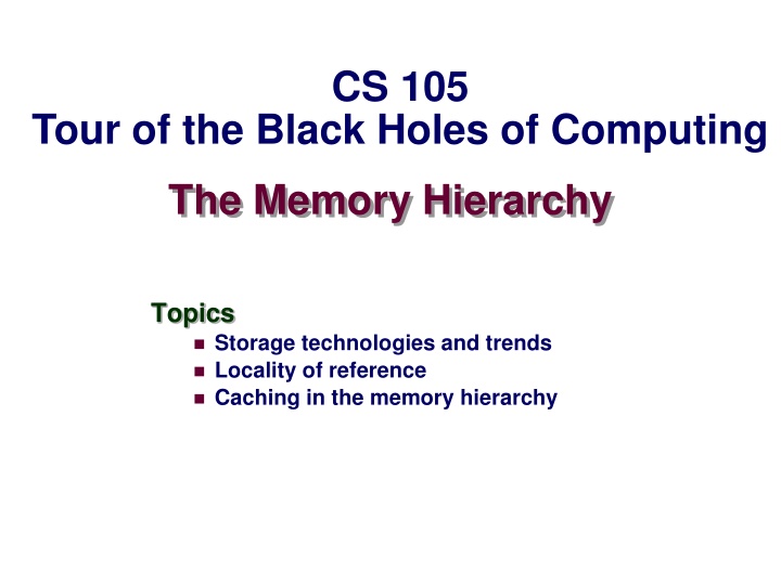
CS 105 Tour of the Black Holes of Computing The Memory Hierarchy Topics Storage technologies and trends Locality of reference Caching in the memory hierarchy
Random-Access Memory (RAM) Key features RAM is traditionally packaged as a chip. Basic storage unit is normally a cell (one bit per cell). Multiple RAM chips form a memory. RAM comes in two varieties: SRAM (Static RAM) DRAM (Dynamic RAM) CS 105 2
SRAM vs DRAM Summary Trans. Access Needs Needs per bit time refresh? EDC? Cost Applications SRAM 4 or 6 1X No Maybe 100x Cache memories DRAM 1 10X Yes Yes 1x Main memories, frame buffers CS 105 3
Traditional Bus Structure Connecting CPU and Memory A bus is a collection of parallel wires that carry address, data, and control signals. Buses are typically shared by multiple devices. CPU chip Register file ALU System bus Memory bus Main memory I/O bridge Bus interface CS 105 5
Memory Read Transaction (1) CPU places address A on the memory bus. Register file Load operation:movq A, %rax ALU %rax Main memory 0 I/O bridge A Bus interface A x CS 105 6
Memory Read Transaction (2) Main memory reads A from the memory bus, retrieves word x, and places it on the bus. Register file Load operation:movq A, %rax ALU %rax Main memory 0 I/O bridge x Bus interface A x CS 105 7
Memory Read Transaction (3) CPU read word x from the bus and copies it into register %rax. Register file Load operation:movq A, %rax ALU %rax x Main memory 0 I/O bridge Bus interface A x CS 105 8
Memory Write Transaction (1) CPU places address A on bus. Main memory reads it and waits for the corresponding data word to arrive. Register file Store operation:movq %rax, A ALU %rax y Main memory 0 I/O bridge A Bus interface A CS 105 9
Memory Write Transaction (2) CPU places data word y on the bus. Register file Store operation:movq %rax, A ALU %rax y Main memory 0 I/O bridge y Bus interface A CS 105 10
Memory Write Transaction (3) Main memory reads data word y from the bus and stores it at address A. Register file Store operation:movq %rax, A ALU %rax y main memory 0 I/O bridge Bus interface A y CS 105 11
Memory Write Transaction (1) CPU places address A on bus. Main memory reads it and waits for the corresponding data word to arrive. Register file Store operation:movq %rax, A ALU %rax y Main memory 0 I/O bridge A Bus interface A CS 105 12
Memory Write Transaction (2) CPU places data word y on the bus. Register file Store operation:movq %rax, A ALU %rax y Main memory 0 I/O bridge y Bus interface A CS 105 13
Memory Write Transaction (3) Main memory reads data word y from the bus and stores it at address A. Register file Store operation:movq %rax, A ALU %rax y main memory 0 I/O bridge Bus interface A y CS 105 14
Reading a Disk Sector (1) CPU chip CPU initiates a disk read by writing a command, logical block number, and destination memory address to a port (address) associated with disk controller. Register file ALU Main memory Bus interface I/O bus USB Graphics adapter Disk controller controller mousekeyboard Monitor Disk CS 105 16
Reading a Disk Sector (2) CPU chip Disk controller reads the sector and performs a direct memory access (DMA) transfer into main memory. Register file ALU Main memory Bus interface I/O bus USB Graphics adapter Disk controller controller MouseKeyboard Monitor Disk CS 105 17
Reading a Disk Sector (3) CPU chip When the DMA transfer completes, the disk controller notifies the CPU with an interrupt (i.e., asserts a special interrupt pin on the CPU) Register file ALU Main memory Bus interface I/O bus USB Graphics adapter Disk controller controller MouseKeyboard Monitor Disk CS 105 18
Solid State Disks (SSDs) I/O bus Requests to read and write logical disk blocks Solid State Disk (SSD) Flash translation layer Flash memory Block 0 Block B-1 Page 0 Page 1 Page 0 Page 1 Page P-1 Page P-1 Pages: 512KB to 4KB, Blocks: 32 to 128 pages Data read/written in units of pages Page can be written only after block has been erased 19 Block wears out after about 100,000 writes CS 105
SSD Performance Characteristics Sequential read tput Random read tput Avg seq read time 550 MB/s 365 MB/s 50 us Sequential write tput Random write tput Avg seq write time 470 MB/s 303 MB/s 60 us Sequential access faster than random access Common theme in the memory hierarchy Random writes are somewhat slower Erasing a block takes a long time (~1 ms) Modifying a block page requires all other pages to be copied to new block In earlier SSDs, the read/write gap was much larger 20 Source: Intel SSD 730 product specification. CS 105
SSD Tradeoffs vs Rotating Disks Advantages No moving parts faster, less power, more rugged Disadvantages Have the potential to wear out Mitigated by wear leveling logic in flash translation layer E.g. Intel SSD 730 guarantees 128 petabyte (128 x 1015 bytes) of writes before they wear out In 2015, about 30 times more expensive per byte Applications MP3 players, smart phones, laptops Beginning to appear in desktops and servers CS 105 21
The CPU-Memory Gap The gap widens between DRAM, disk, and CPU speeds. 100,000,000.0 10,000,000.0 Disk 1,000,000.0 SSD 100,000.0 Disk seek time SSD access time DRAM access time SRAM access time CPU cycle time Effective CPU cycle time 10,000.0 1,000.0 Time (ns) DRAM 100.0 10.0 1.0 CPU 0.1 0.0 1985 1990 1995 2000 2003 2005 2010 2015 Year CS 105 22
Locality to the Rescue! The key to bridging this CPU-Memory gap is a fundamental property of computer programs known as locality CS 105 23
Locality Principle of Locality: Programs tend to use data and instructions with addresses near or equal to those they have used recently Temporal locality: Recently referenced items are likely to be referenced again in the near future Spatial locality: Items with nearby addresses tend to be referenced close together in time CS 105 24
Locality Example sum = 0; for (i = 0; i < n; i++) sum += a[i]; return sum; Data references Reference array elements in succession (stride-1 reference pattern). Reference variable sum each iteration. Spatial locality Temporal locality Instruction references Reference instructions in sequence. Cycle through loop repeatedly. Spatial locality Temporal locality CS 105 25
Qualitative Estimates of Locality Claim: Being able to look at code and get a qualitative sense of its locality is a key skill for a professional programmer. Question: Does this function have good locality with respect to array a? int sum_array_rows(int a[M][N]) { int i, j, sum = 0; for (i = 0; i < M; i++) for (j = 0; j < N; j++) sum += a[i][j]; return sum; } CS 105 26
Locality Example Question: Does this function have good locality with respect to array a? int sum_array_cols(int a[M][N]) { int i, j, sum = 0; for (j = 0; j < N; j++) for (i = 0; i < M; i++) sum += a[i][j]; return sum; } CS 105 27
Locality Example Question: Can you permute the loops so that the function scans the 3-d array a with a stride-1 reference pattern (and thus has good spatial locality)? int sum_array_3d(int a[M][N][N]) { int i, j, k, sum = 0; for (i = 0; i < M; i++) for (j = 0; j < N; j++) for (k = 0; k < N; k++) sum += a[k][i][j]; return sum; } CS 105 28
Memory Hierarchies Some fundamental and enduring properties of hardware and software: Fast storage technologies cost more per byte and have less capacity Gap between CPU and main memory speed is widening Well-written programs tend to exhibit good locality These fundamental properties complement each other beautifully They suggest an approach for organizing memory and storage systems known as a memory hierarchy CS 105 29
An Example Memory Hierarchy Smaller, faster, and costlier (per byte) storage devices L0: registers CPU registers hold words retrieved from L1 cache on-chip L1 cache (SRAM) L1: L1 cache holds cache lines retrieved from the L2 cache memory off-chip L2 cache (SRAM) L2: L2 cache holds cache lines retrieved from main memory main memory (DRAM) L3: Larger, slower, and cheaper (per byte) storage devices Main memory holds disk blocks retrieved from local disks local secondary storage (local disks) L4: Local disks hold files retrieved from disks on remote network servers remote secondary storage (distributed file systems, Web servers) L5: CS 105 30
Caches Cache: Smaller, faster storage device that acts as staging area for subset of data in a larger, slower device Fundamental idea of a memory hierarchy: For each k, the faster, smaller device at level k serves as cache for larger, slower device at level k+1 Why do memory hierarchies work? Programs tend to access data at level k more often than they access data at level k+1 Thus, storage at level k+1 can be slower, and thus larger and cheaper per bit Big Idea: Large pool of memory that costs as little as the cheap storage near the bottom, but serves data to programs at rate of the fast storage near the top CS 105 31
General Cache Concepts Smaller, faster, more expensive memory caches a subset of the blocks Cache 8 4 9 14 10 3 Data is copied in block-sized transfer units 4 10 Larger, slower, cheaper memory viewed as partitioned into blocks Memory 0 1 2 3 4 4 5 6 7 8 9 10 10 11 12 13 14 15 CS 105 32
General Cache Concepts: Hit Data in block b is needed Request: 14 Block b is in cache: Hit! Cache 8 9 14 14 3 Memory 0 1 2 3 4 5 6 7 8 9 10 11 12 13 14 15 CS 105 33
General Cache Concepts: Miss Data in block b is needed Request: 12 Block b is not in cache: Miss! Cache 8 9 12 14 3 Block b is fetched from memory Request: 12 12 Block b is stored in cache Placement policy: determines where b goes Replacement policy: determines which block gets evicted (victim) Memory 0 1 2 3 4 5 6 7 8 9 10 11 12 12 13 14 15 CS 105 34
General Caching Concepts: Types of Cache Misses Cold (compulsory) miss Cold misses occur because the cache is empty. Conflict miss Most caches limit blocks at level k+1 to a small subset (sometimes a singleton) of the block positions at level k E.g. Block i at level k+1 must go in block (i mod 4) at level k Conflict misses occur when the level k cache is large enough, but multiple data objects all map to the same level k block E.g. Referencing blocks 0, 8, 0, 8, 0, 8, ... would miss every time Capacity miss Occurs when set of active cache blocks (working set) is larger than the cache CS 105 35
Examples of Caching in the Memory Hierarchy Cache Type What Cached Where Cached Latency (cycles) Managed By Registers 8-byte word CPU registers 0 Compiler TLB Address translations 32-byte block On-Chip TLB 0 Hardware L1 cache On-Chip L1 Off-Chip L2 Main memory 1 Hardware Hardware Hardware+ OS L2 cache 32-byte block 10 100 Virtual Memory 4-KB page Buffer cache Parts of files Main memory Local disk 100 OS AFS/NFS client Network buffer cache Parts of files 10,000,000 Browser cache Web pages Local disk 10,000,000 Web browser Web proxy server Web cache Web pages Remote server disks 1,000,000,000 CS 105 36

")


")
")
")
")
")
")
")
")
")
")
")
")
")