Microelectronic System Design Tips for CMOS Inverter Layout Optimization
Download Presenatation

Explore step-by-step guidance on optimizing the layout of a CMOS inverter for efficient performance in microelectronic system design. Learn about contact placement, active margin, gate connections, and more to enhance functionality.

Uploaded on | 0 Views
Download Presentation
Please find below an Image/Link to download the presentation.
The content on the website is provided AS IS for your information and personal use only. It may not be sold, licensed, or shared on other websites without obtaining consent from the author. If you encounter any issues during the download, it is possible that the publisher has removed the file from their server.
You are allowed to download the files provided on this website for personal or commercial use, subject to the condition that they are used lawfully. All files are the property of their respective owners.
The content on the website is provided AS IS for your information and personal use only. It may not be sold, licensed, or shared on other websites without obtaining consent from the author.
E N D
Presentation Transcript
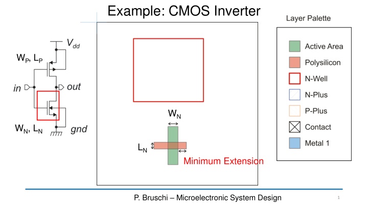
Example: CMOS Inverter WP, LP WN WN, LN LN Minimum Extension P. Bruschi Microelectronic System Design 1
Let's introduce a contact WP, LP WN, LN Contact Exact width P. Bruschi Microelectronic System Design 2
Then, we provide enough active surround to the contact WP, LP WN, LN Contact to active margin P. Bruschi Microelectronic System Design 3
Then, we provide enough active surround to the contact WP, LP WN, LN Poly-Active spacing Contact to poly-gate minum spacing P. Bruschi Microelectronic System Design 4
Place the n-MOS as close as possible to the n-well WP, LP Minimum active to well spacing WN, LN P. Bruschi Microelectronic System Design 5
Now draw the p-MOS inside the n-well WP WP, LP LP Extension poly of active WN, LN P. Bruschi Microelectronic System Design 6
Place the source/drain contact of the WP, LP Extension active of poly Contact to poly-gate spacing WN, LN P. Bruschi Microelectronic System Design 7
Reduce the active extension to the minimum WP, LP Extension active of poly (minimum) WN, LN P. Bruschi Microelectronic System Design 8
Connect the gates of the n-MOS and p-MOS WP, LP Minimum Active to n-well margin WN, LN Minimum poly to active spacing Minimum poly width P. Bruschi Microelectronic System Design 9
Introduce the metal-1 connections WP, LP Minimum metal1 to metal1 spacing Minimum metal1 width WN, LN Metal 1 to contact overlap P. Bruschi Microelectronic System Design 10
Introduce the substrate and n-well contacts Minimum active to active spacing WP, LP Minimum poly to active spacing WN, LN Minimum active to active spacing P. Bruschi Microelectronic System Design 11
Resize the n-well to comply with all active margins. Connect sources to bodies WP, LP Minimum active to well margin WN, LN P. Bruschi Microelectronic System Design 12
Cover all n-plus active areas with n-plus implant well contact WP, LP well contact Minimum n-plus overlap of active areas drain/source implants WN, LN P. Bruschi Microelectronic System Design 13
Same thing with p-plus active areas (p-plus implant) WP, LP drain/source implants Minimum n-plus overlap of active areas substrate contact WN, LN substrate contact P. Bruschi Microelectronic System Design 14
Same thing with p-plus active areas (p-plus implant) WP, LP Minimum n-plus to p-plus spacing WN, LN P. Bruschi Microelectronic System Design 15
Create a poly-metal1 contact if required WP, LP WN, LN Margin of contact to poly on every-side P. Bruschi Microelectronic System Design 16
Create a poly-metal1 contact if required WP, LP WN, LN P. Bruschi Microelectronic System Design 17


")
")